This demand is driven by the rapid growth of AI applications. Strategically located in the Grenoble area, one of Europe’s most established semiconductor clusters, the site strengthens Merck’s role in building a more resilient and competitive European semiconductor ecosystem.
“Increasing chip performance is increasingly dependent on the complex architecture of chip systems rather than miniaturization alone. As chip designs become more complex, even the smallest irregularities can jeopardize entire systems. This makes quality assurance and reliability more challenging than ever,” said Ben Hein, Member of the Executive Board of Merck and CEO Electronics. “Our metrology and inspection expertise provides chipmakers with the precise tools and solutions they need to realize the next wave of technological advances.”
Enabling next-generation innovation in semiconductors
The new facility quintuples Merck’s production capacity for metrology and inspection tools. These solutions are becoming increasingly important to ensure accuracy and defect detection in chip manufacturing and support chip manufacturers in advanced packaging solutions and heterogeneous integration. These 3D technologies for next-generation chip architectures bring memory and logic chips closer together through vertical stacking, increasing performance while reducing energy consumption.
Measurement tools measure critical chip manufacturing parameters such as depths, step heights and thicknesses, enabling real-time adjustments that improve process control. Inspection tools detect a variety of defect types and ensure the highest quality standards. Together, these technologies increase manufacturing yields, reduce production costs and accelerate time-to-market for next-generation semiconductor innovations.
Driving sustainable growth
Merck’s Electronics business is a key enabler of technology roadmaps and offers one of the broadest portfolios of materials and equipment for the semiconductor industry. The acquisition of Unity-SC, based in Montbonnot-Saint-Martin near Grenoble, France, in October 2024 has further complemented Merck’s optical expertise. With now more than 100 employees at the new site – working in both production and research and development – and plans to create around 100 more highly skilled engineering positions over the next four years, Merck is driving the convergence of optics and semiconductors to meet the demands of next-generation technologies. This will enable advanced chip systems for AI, High-Performance Computing (HPC) and High-Bandwidth Memory (HBM) applications, strengthening Merck Electronics’ path to profitable growth.
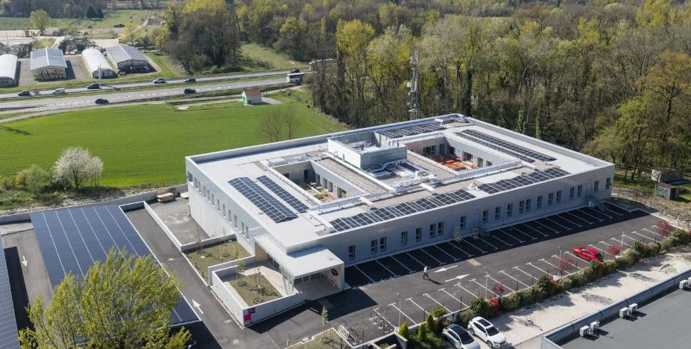
The Saint-Ismier site is an example of Merck’s commitment to sustainability. It features a wooden structure insulated with straw, a hermetic concrete base and photovoltaic panels on the roof, as well as parking lot canopies to generate renewable energy, which cover around 40% of the site’s energy consumption. Inside, bright courtyards, adjustable solar shading devices and a cooling underfloor heating system ensure an energy-efficient and comfortable workspace.
– – – – –
Further links
👉 www.merckgroup.com
Photos: Merck