The electrical characterization of thin films typically requires a sequence of additional post-deposition processing steps, including photolithography, pattern transfer and mask removal. These steps add time and complexity and can limit compatibility with certain materials.
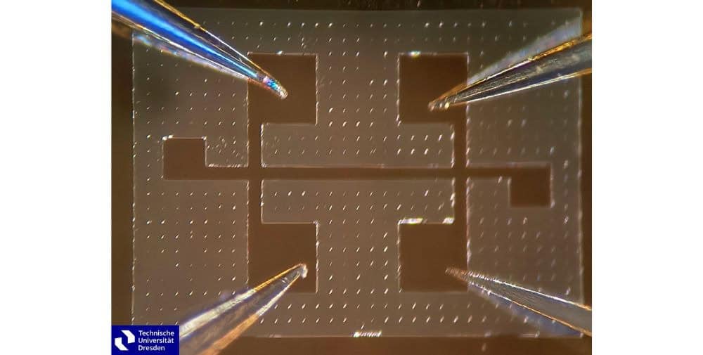
The new embedded silicon test structure from Chipmetrics introduces a lift-off style measurement approach that completely bypasses these requirements.
With the Chipmetrics structure, researchers can go directly from deposition to measurement in minutes.
Key benefits include:
- No photolithography or etching required
- Compatible with virtually any thin-film material
- Immediate electrical testing after deposition
- Customizable layouts for application-specific measurements
By eliminating multiple fabrication steps, the structure significantly reduces the time required to acquire electrical data during thin-film process development.
Proven measurement capability
The electrical test structure was validated in collaboration with the TU Dresden, Chair of Nanoelectronics (Prof. Martin Knaut).
In initial experiments, the structure was used to measure the electrical properties of an 8.7 nm thick PEALD-TiN film deposited on 46 nm Al²O³ using a four-point probe measurement configuration.
These tests confirmed that the structure enables accurate measurement of sheet resistance and resistivity, demonstrating its suitability for the characterization of advanced thin films.
Broad range of electrical characterization capabilities
The test structure supports a variety of electrical measurements, including:
- Film resistance and resistivity
- Contact resistance
- Hall coefficient measurements
- Temperature coefficient of resistance (TCR)
- Magnetoresistance
- Electromigration testing
IV-Linearity and self-heating characterization
This versatility makes the structure valuable for both academic research environments and semiconductor process development laboratories.
Accelerating material and process development
As semiconductor devices continue to be miniaturized and new materials are introduced, fast electrical feedback is becoming increasingly important.
By eliminating post-deposition patterning steps, the Chipmetrics test structure enables researchers to evaluate the electrical performance of new materials and deposition processes faster than ever before.
About Chipmetrics
Chipmetrics Oy develops and supplies metrology solutions for manufacturing processes in the semiconductor industry, focusing on innovative measurement chips and ALD measurement services. The main product is the PillarHall® measurement chip for near-instant conformance measurement of thin film processes. Founded in 2019, the company is headquartered in Joensuu, Finland, and has employees and sales partners in Japan, South Korea, the USA and Germany.
– – – – – – –
Further links
👉 www.chipmetrics.com
Photo: TU Dresden