21.04.2026. Top-class contributions and a sold-out location show: To keep value creation in Europe in the long term, everyone must pull together!
Categories
21.04.2026. Top-class contributions and a sold-out location show: To keep value creation in Europe in the long term, everyone must pull together!
Categories
Tags
Contact info
Silicon Saxony
Marketing, Kommunikation und Öffentlichkeitsarbeit
Manfred-von-Ardenne-Ring 20 F
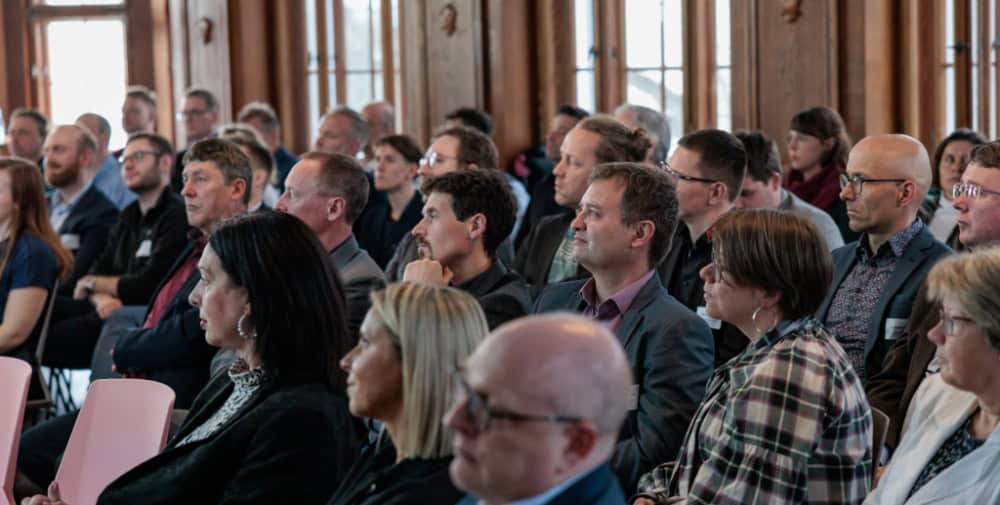
On April 21, around 70 participants from SMEs, large companies, research and universities came together at the Chemnitz Technology Campus to establish chip.space, a new exchange format for microelectronics. The interest in the event, which was organized by Silicon Saxony, the City of Chemnitz and the Chemnitz Microelectronics and Microsystems Technology Association, was so great that the event was fully booked.
At the very beginning, Sven Schulze, Lord Mayor of the City of Chemnitz, emphasized the importance of microelectronics as a key technology. He was supported by business promoters from Chemnitz and the Ore Mountains as well as representatives of the Chemnitz Chamber of Industry and Commerce, who all agreed that it must be a common goal to keep microelectronics value creation in Europe in the long term.
Despite considerable investment and various initiatives, Europe will not succeed in achieving the goal of a 20% market share in international semiconductor production by 2030. In order to strengthen European competitiveness despite this, regional cooperation must be strengthened, skills promoted and key aspects of value creation established and expanded in addition to efforts at European and national level.
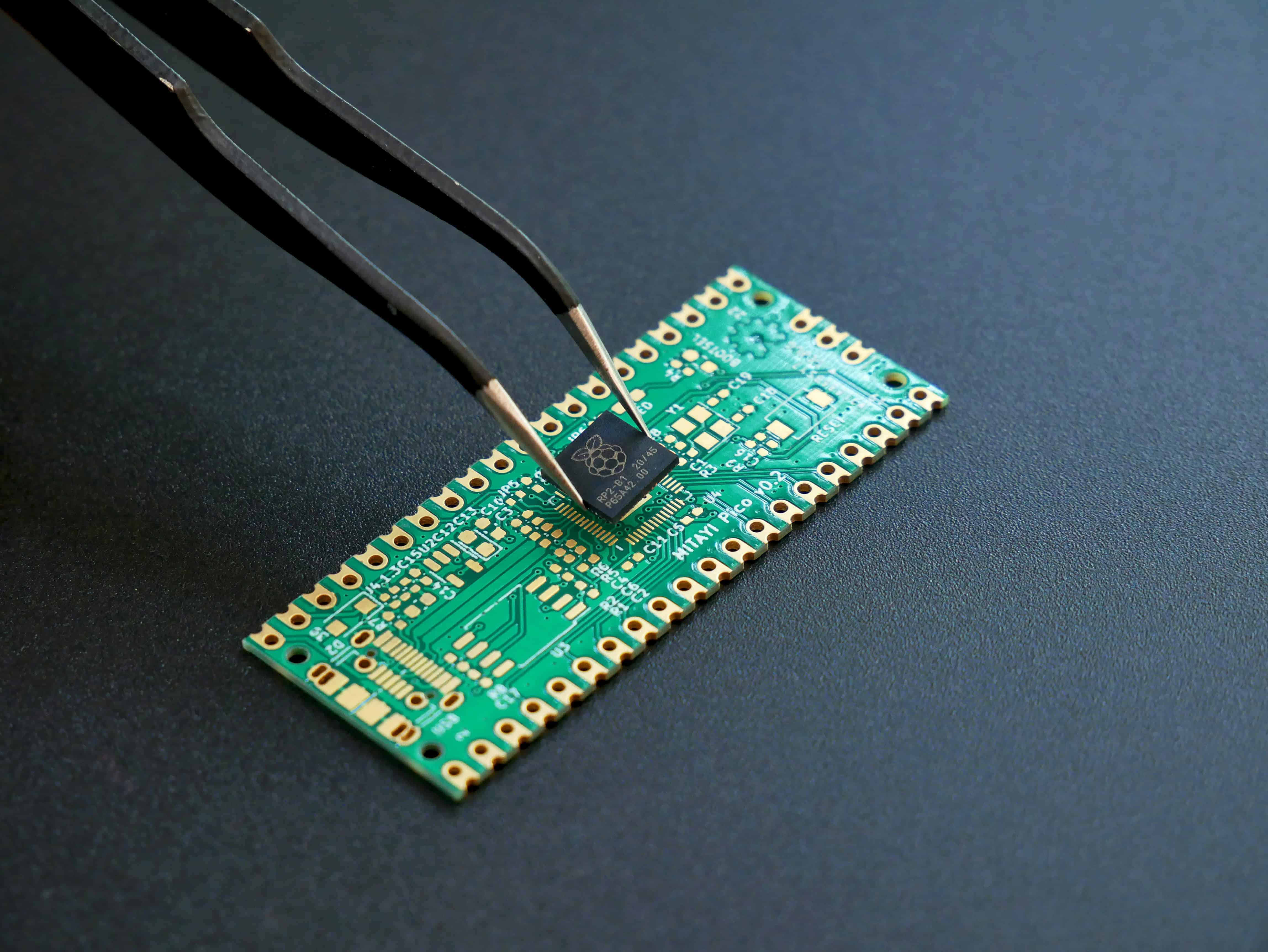
The contributions under the motto “From the idea to the chip – value creation in microelectronics” therefore consistently followed the entire value chain: from chip design (electronics and MEMS) to front-end and back-end production (including assembly, packaging and testing) through to application.
The program was supplemented by pitches from regional and Saxon companies as well as from research and development. Among them:
“The presentations provided the right impetus for a lively subsequent discussion – in many cases, the ice was broken and new ideas for future joint initiatives emerged,” emphasized Dr. Detlef Billep, Managing Director of EDC Electronic Design Chemnitz GmbH and Chairman of the Förderverein für Mikroelektronik und Mikrosystemtechnik Chemnitz e.V.
.
All in all, several speakers from industry and research provided practical insights that showed, among other things, the extent to which technologies, skills and roles are currently shifting. In general, more and more value creation is being mapped locally again, both for SMEs and large companies.
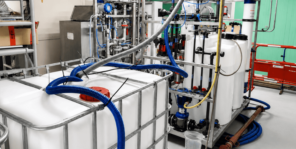
Wafer fabs such as X-FAB, for example, are starting to offer additional steps such as heterointegration or wafer-level packaging (3D integration) alongside chip production itself. At the same time, fabless companies such as EDC Electronic Design Chemnitz GmbH are expanding their service portfolio to include wafer-level and final testing. This has two clear advantages: On the one hand, the entire chip know-how remains more in-house, while at the same time new service offerings are created. Collaborations – for example with the Test & Reliability Center at Fraunhofer ENAS and with SMEs such as SweepMe! and i-ROM – will continue to gain in importance in the short, medium and long term.
Prof. Jan Mehner, Managing Director of i-ROM, explained how electronics and MEMS design, which previously took place in different program systems, can be intelligently combined. Simulations and sensitivity analyses provide important characteristic values for evaluating production tolerances and enable statements to be made about the yield and drift behavior of sensors.
Dr. Gabriel Kittler, CEO Site Erfurt X-FAB MEMS Foundry, spoke in his presentation about the “century of photons”, in which electronics and photonics are key technologies for overcoming current challenges. These are made possible by heterointegration, microtransfer printing of photonic chiplets and advanced materials, among other things.
The role that packaging plays in Europe was also central, because with a share of less than three percent of the global assembly and test market, it is important to find ways to strengthen this added value in Europe – which brings us full circle to the presentation by X-FAB, which already integrates parts of advanced packaging itself. The pointed message from Steffen Kroehnert, Managing Director of ESPAT-Consulting, was: “No chips without package.”
And because it is extremely important for the success of a location that innovations “Made in Saxony” can also be scaled internationally, Peter Kalinowski from u-blox used a positive example to show how the IP of the TU Chemnitz spin-off NAVENTIK is now being incorporated into global GNSS platforms.
It was above all the personal exchange that characterized the event. The discussions deliberately took place after the presentations – at eye level and with plenty of room for new ideas.
The city of Chemnitz also emphasized: “chip.space has created concrete points of contact for cooperation. Now we need to further network the existing competencies and translate them into concrete added value for the location.”
The successful launch has now laid the foundation: chip.space is to be held as an annual format in future and be a platform for exchange, cooperation and innovation in a key industry in Europe.
You need to load content from reCAPTCHA to submit the form. Please note that doing so will share data with third-party providers.
More InformationYou are currently viewing a placeholder content from Turnstile. To access the actual content, click the button below. Please note that doing so will share data with third-party providers.
More InformationYou are currently viewing a placeholder content from Facebook. To access the actual content, click the button below. Please note that doing so will share data with third-party providers.
More InformationYou are currently viewing a placeholder content from Google Maps. To access the actual content, click the button below. Please note that doing so will share data with third-party providers.
More InformationYou are currently viewing a placeholder content from OpenStreetMap. To access the actual content, click the button below. Please note that doing so will share data with third-party providers.
More InformationYou are currently viewing a placeholder content from Instagram. To access the actual content, click the button below. Please note that doing so will share data with third-party providers.
More InformationYou are currently viewing a placeholder content from X. To access the actual content, click the button below. Please note that doing so will share data with third-party providers.
More Information