Testing is no longer just about finding defects
For decades, semiconductor testing was often seen as a quality control step, a necessary process to identify faulty components before they reached customers. Today, testing is much more than a final quality check.
As components become more complex and expensive to manufacture, the knowledge gained through testing has become as valuable as the manufacturing process itself. The data collected during wafer testing helps manufacturers make more informed decisions about yield, performance and production costs long before the components reach the market.
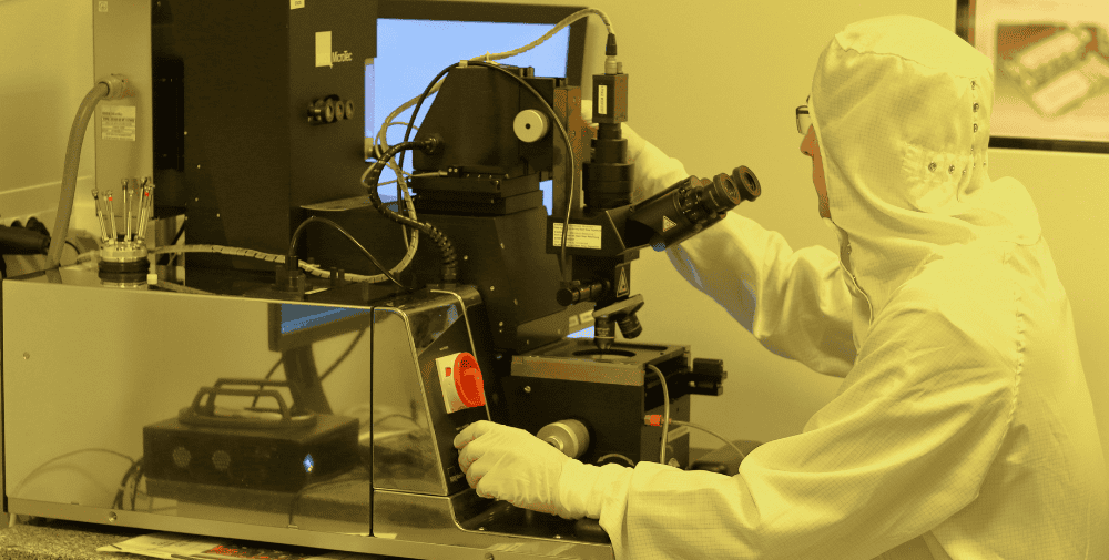
At the wafer level, individual chips are electrically tested before packaging to identify defects and verify functionality. Detecting problems early helps manufacturers improve yields while avoiding the significant costs associated with packaging and assembly.
With state-of-the-art components, testing is no longer just about determining whether a chip passes or fails the test. It has become a critical tool for understanding device behavior, optimizing manufacturing processes and ensuring long-term reliability.
Why HBM is raising the bar
Few technologies exemplify this shift better than High Bandwidth Memory.
HBM has become essential for AI accelerators and HPC systems because it offers significantly higher memory bandwidth while consuming less power. To achieve this performance, multiple memory chips must be stacked vertically and interconnected using advanced packaging technologies.
The challenge is that when stacking multiple chips, even a single defect can have costly consequences. If one chip within an HBM stack fails, the entire package can be compromised. As memory stacks become more complex, manufacturers are under increasing pressure to ensure that every component entering assembly is fully functional.
This is where known-good-die (KGD) strategies and wafer-level testing become essential.
By validating chips prior to packaging, manufacturers can:
- improve overall yield
- reduce assembly costs
- minimize costly failures in downstream processes
- increase confidence in final system performance
Verifying these devices also requires a new level of precision as engineers work at higher speeds, tighter tolerances and increasingly demanding performance targets.
The result is a growing need for advanced test and measurement capabilities that can keep pace with the demands of AI-driven computing.
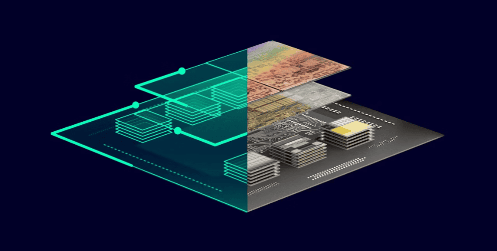
Advanced packaging techniques pose new test challenges
Advanced packaging techniques and chiplet-based designs solve key performance challenges, but also make testing significantly more complicated.
Instead of integrating everything on a single monolithic chip, modern systems increasingly combine multiple specialized chips in a single package. This approach offers flexibility and performance benefits, but brings new challenges for validation and characterization.
Engineers now need to understand not only how each chip works individually, but also how they work together once integrated into a single package.
This means that test strategies must consider:
- More interfaces and connections
- The communication and performance between chips
- Package-level interactions
- System-level reliability
As more and more functions are integrated at the package level, testing becomes deeper, more comprehensive and more data-intensive.
According to Slessor, this trend is fundamentally changing how the industry thinks about testing. Rather than a single manufacturing step, testing is becoming a continuous source of insight throughout the lifecycle of semiconductors.
The rise of photonics and electro-optical testing
Another important topic discussed in the podcast was the increasing adoption of silicon photonics and co-packaged optics.
As AI infrastructure scales, traditional electrical interconnects are increasingly reaching their limits in terms of bandwidth and power supply. Optical technologies offer a path forward by enabling faster and more efficient data transfer between processors, memory and network devices.
However, the introduction of optics into semiconductor systems creates entirely new testing requirements.
Unlike traditional semiconductor devices, photonic systems require both electrical and optical performance to be validated simultaneously. This brings challenges such as:
- Precise optical alignment
- Signal coupling and calibration
- Electro-optical characterization
- Additional validation at wafer, die and system level
As photonics makes the leap from research to production, manufacturers need test solutions that can combine optical and electrical measurements in a unified workflow.
Merging optical and electrical testing represents a major shift in the way semiconductor devices are characterized and validated.
Testing becomes a competitive advantage
What unites AI, HBM, advanced packaging techniques and photonics is the growing complexity of manufactured devices. Each new technology brings with it significant performance improvements, but also presents new challenges in manufacturing and validation. As a result, testing is no longer just a checkpoint at the end of production.
Companies that can test more effectively gain a significant advantage in both manufacturing efficiency and product performance.
The ability to detect problems earlier, optimize yields, reduce costs and accelerate product qualification is becoming increasingly important as innovation in the semiconductor space continues to accelerate.
For many companies, advanced test capabilities are now directly linked to business success.
Looking to the future
The future of semiconductor innovation will depend on much more than just shrinking the size of transistors. AI-driven computing, HBM, advanced packaging techniques, chiplets and silicon photonics are creating entirely new system architectures and posing entirely new challenges for test engineering.
As Mike Slessor explains on the Semiconductor Leadership Podcast, the industry’s ability to manage this growing complexity will play a critical role in future success.
Companies that invest in advanced test capabilities today will be better equipped to deliver the performance and reliability that next-generation AI, HPC and networking systems require.
As these technologies evolve, semiconductor test will play an increasingly important role in enabling the breakthroughs that will shape the next era of computing.
– – – – –
Further links
👉 www.formfactor.com
Photo: unsplash