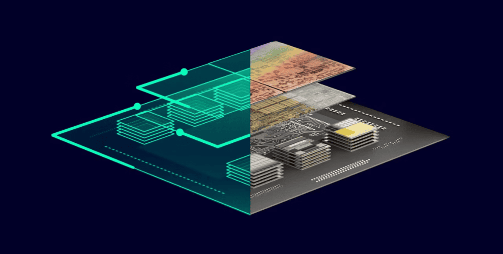
Building on this experience, Evatec is now expanding its technology roadmap from wafer-based processes to panel formats from 310 x 310 millimeters, which can be further scaled up to sizes of 650 x 650 millimeters. These developments focus on key applications such as redistribution layers, backside metallization, through-glass via technologies and plasma-based etch processes for advanced substrates.
For redistribution layer and backside metallization processes, Evatec has started a special development project based on the CLUSTERLINE® 300 platform. The modified system is designed to process panels efficiently while increasing substrate utilization per cycle. This enables higher throughput and lower cost per chip and supports larger AI chiplets and advanced memory integration. New sputtering and etching modules, improved sources and in-situ process control are under development to ensure high uniformity and optimized material consumption.
Glass-based interposers are also gaining importance in RF and RF packaging. Evatec is preparing its CLUSTERLINE® 600 platform for thin film deposition on large glass panels, with a roadmap that includes adhesion layers and copper seed layers for through-glass vias with increasing aspect ratios. Ionized plasma features enable conformal coverage along via sidewalls for reliable interconnect performance.
In parallel, Evatec is expanding its portfolio to include reactive ion etch and desmear solutions for organic and glass substrates. These developments aim to provide scalable and production-ready solutions that meet the evolving needs of advanced panel-level packaging.
– – – – – –
Further links
👉 https://evatecnet.com
Photo: evatec