Topological phenomenon in a semiconductor component
Semiconductor components are the smallest switching units and ensure that electrons can be transported and controlled in modern electronics. This is what makes our everyday technologies work – cell phones and laptops as well as modern medical technology and car sensors. However, material impurities or temperature fluctuations can disrupt the flow of electricity in these sensitive components. The functionality of the respective electronic device then suffers.
Theoretical and experimental physicists from the Würzburg-Dresden Cluster of Excellence ct.qmat – Complexity and Topology in Quantum Matter have now succeeded in jointly developing a semiconductor component made of aluminum gallium arsenide (AlGaAs) in which a topological quantum phenomenon protects the interference-prone electron flow. The research results were published in the journal Nature Physics.
“Thanks to the topological skin effect, the currents between the various contacts on the quantum semiconductor cannot be disturbed by impurities or other external influences. This makes topological components increasingly interesting for the semiconductor industry. This is because the extremely high degrees of material purity that make today’s electronics so expensive can be dispensed with in their production,” explains Prof. Jeroen van den Brink, Director at the Leibniz Institute for Solid State and Materials Research Dresden (IFW) and founding member of ct.qmat. Topological quantum materials are considered to be extremely robust and are therefore particularly suitable for extremely power-hungry technologies. “Our quantum semiconductor is stable and highly precise at the same time – this combination is unusual. This makes our topological component particularly exciting for sensor technology.”
Extremely robust & ultra-precise
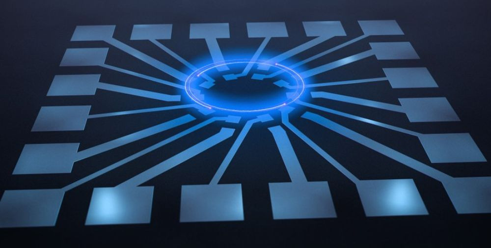
By using the topological skin effect, new types of high-performance electronic quantum components are possible, which can also become very small: “The diameter of our topological quantum component is around 0.1 millimetres and can easily be made even smaller for future electronics applications,” says van den Brink. The research success of the Dresden-Würzburg physics team is that they were the first to realize the topological skin effect on a microscopic level in a semiconductor material. This quantum phenomenon was first experimentally demonstrated at a macroscopic level three years ago – but only in an artificial metamaterial and not in a natural material. Only the current research contribution led to a tiny semiconductor-based topological quantum device that combines extraordinary resistance and ultra-high sensitivity.
“In our quantum device, the relationship between current and voltage is protected by the topological skin effect because the electrons are all at the edge. Even with impurities in the semiconductor material, the current flow remains stable. At the same time, even the slightest fluctuations in current or voltage can be measured by the contacts,” explains van den Brink. The topological quantum component is particularly suitable for the construction of high-precision sensors or amplifiers with a very small diameter.
Clever experimental design
The key to the research success was the idea of provoking the topological effect through a clever arrangement of materials and contacts on an AlGaAs semiconductor component under ultracold temperatures and a strong magnetic field: “We really teased the topological skin effect out of the component,” says van den Brink. To do this, the physics team used a two-dimensional semiconductor structure. The contacts were arranged in such a way that the electrical resistance could be measured at the edges of the contacts and the topological effect could be directly detected there.
Discovering new things across locations
Since 2019, the Cluster of Excellence ct.qmat in Würzburg and Dresden has been researching topological quantum materials that reveal surprising phenomena under extreme laboratory conditions such as ultra-low temperatures, high pressure or strong magnetic fields.
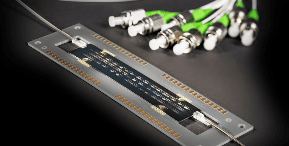
The current research results were also developed by scientists who are at home at both cluster locations. Both theoretical physicists from the University of Würzburg and theoretical and experimental researchers from Dresden were involved in the new quantum device, which was designed at the IFW. After being manufactured in France, the component was tested in Dresden. Jeroen van den Brink and his colleagues are continuing to work on understanding this phenomenon in order to make it usable for future technologies.
Publication
Non-Hermitian topology in a multi-terminal quantum Hall device
Ochkan, K., Chaturvedi, R., Könye, V. et al. Nat. Phys. (2024).
https://www.nature.com/articles/s41567-023-02337-4
Cluster of Excellence ct.qmat
The Cluster of Excellence ct.qmat – Complexity and Topology in Quantum Matter has been jointly funded by Julius-Maximilians-Universität (JMU) Würzburg and Technische Universität (TU) Dresden since 2019. More than 300 scientists from more than 30 countries and four continents are researching topological quantum materials that reveal surprising phenomena under extreme conditions such as ultra-low temperatures, high pressure or strong magnetic fields. The Cluster of Excellence is funded as part of the Excellence Strategy of the German federal and state governments – the only cluster in Germany that spans several federal states.
Contact
Prof. Jeroen van den Brink
Leibniz Institute for Solid State and Materials Research Dresden
Tel.: +49 351 4659-380
Email: j.van.den.brink@ifw-dresden.de
– – – – –
Further links
👉 www.tu-dresden.de
Photo: Christoph Mäder/pixelwg