
Silicon Saxony Alumni Microelectronics
The microelectronics sector in Saxony has a long tradition, and following major structural upheavals—particularly those related to German reunification and the end of the GDR—it is thriving more than ever. Because the future is always rooted in the past, we have made it our mission to pool knowledge, preserve history, and give it a face—or rather, many faces.
That is why we founded Silicon Saxony Alumni, whose members met and exchanged ideas for the first time on October 26, 2022.
Specific topics and regular communication
Our goal is to build an alumni network that can be involved in the following areas in the future:
- Support for the Technical Collections in cataloging historical documents, photographs, and artifacts*
- A Collection of Ideas for Promoting the Preservation of Historical Artifacts and Documents
- Involvement in the area of youth development
- A discussion about fascinating stories from 60 years of microelectronics in Saxony that we can share in our media or with interested members of the press.
* We are looking for people who can provide meaningful insights into specific exhibits, as well as those who moved to Saxony after 1990 and are willing to reflect on their perspective at that time.
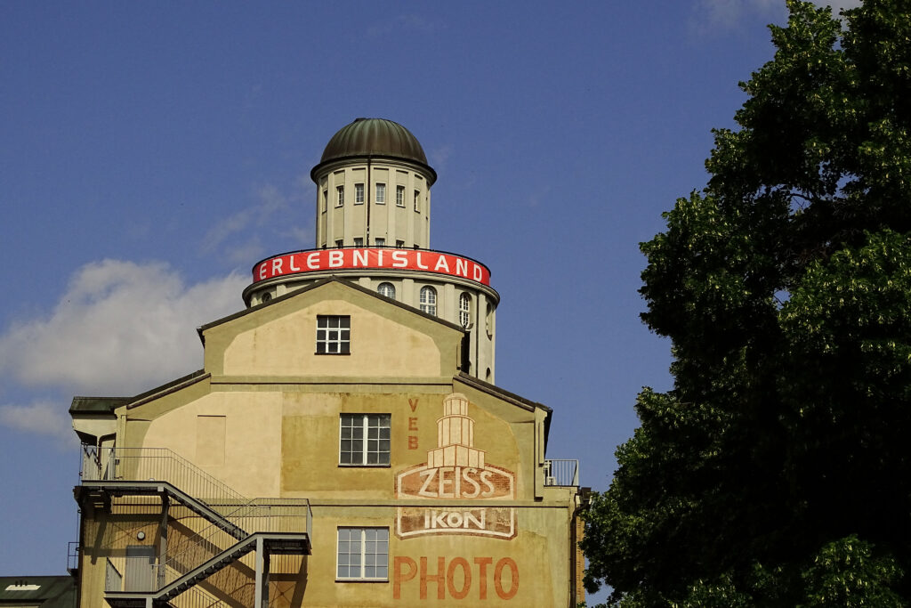
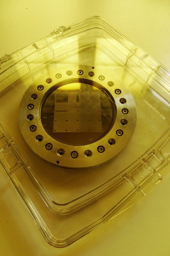
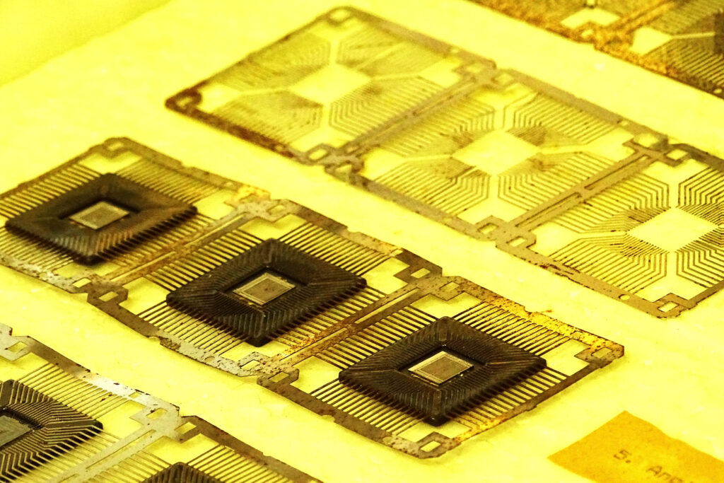
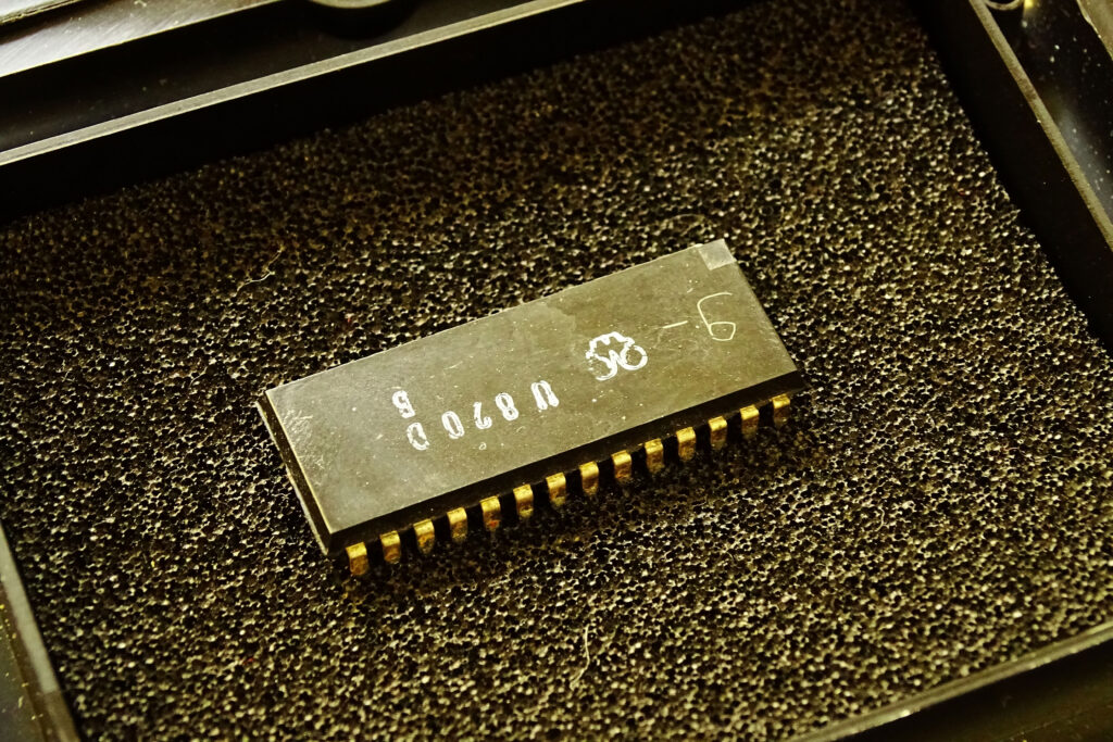
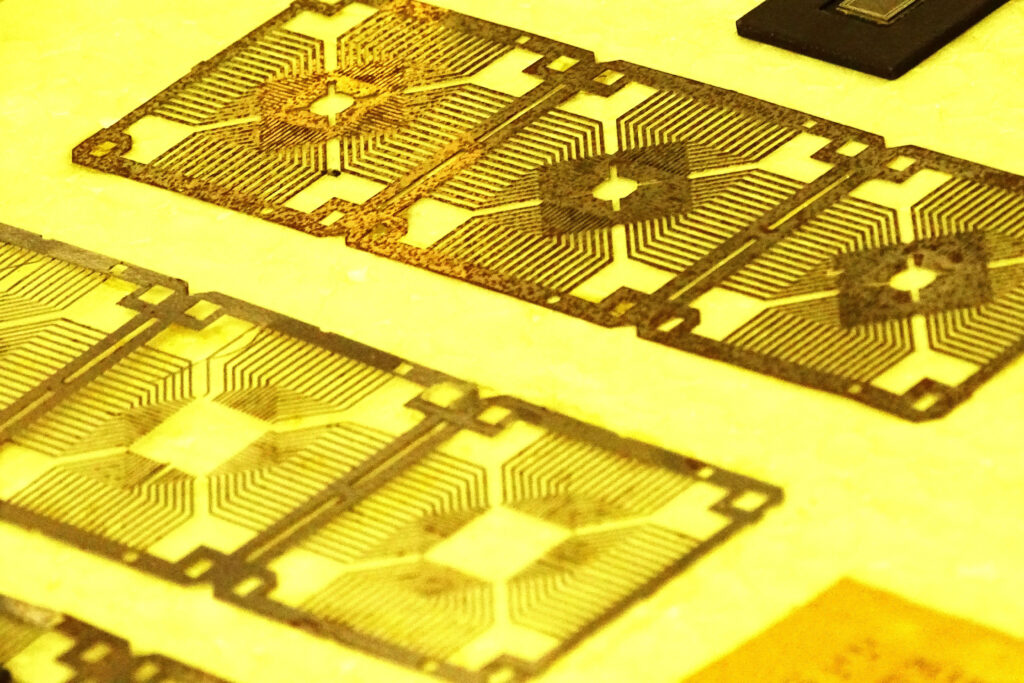
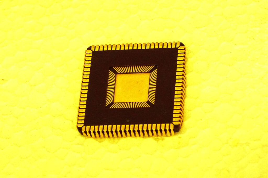
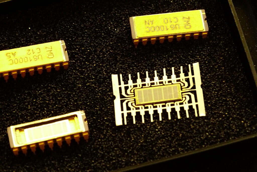
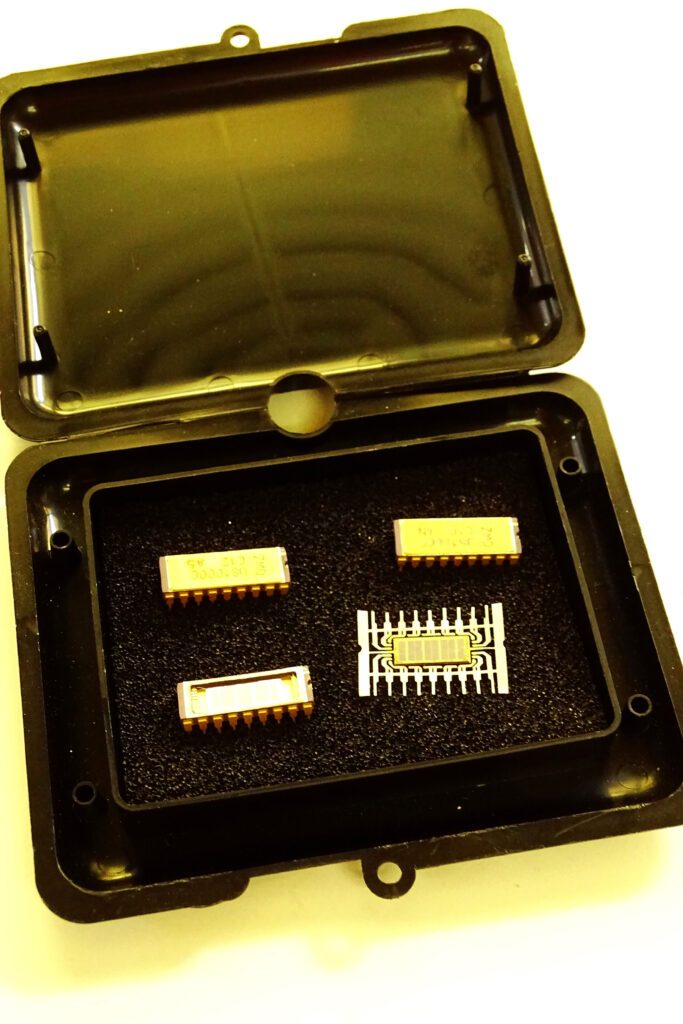
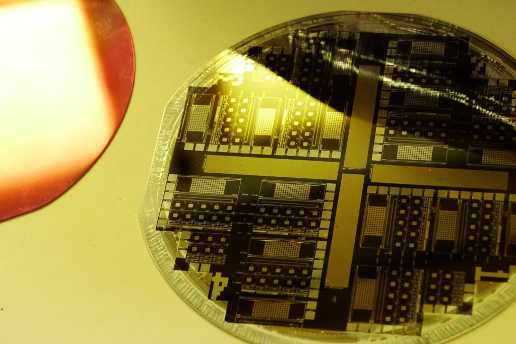
Collection of artifacts from the history of microelectronics


Review
From UV to EUV – ZEISS’s Journey to the Forefront of Lithography Optics
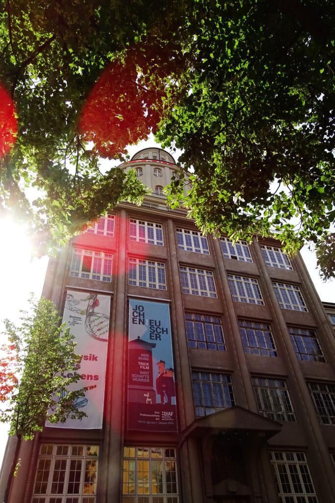
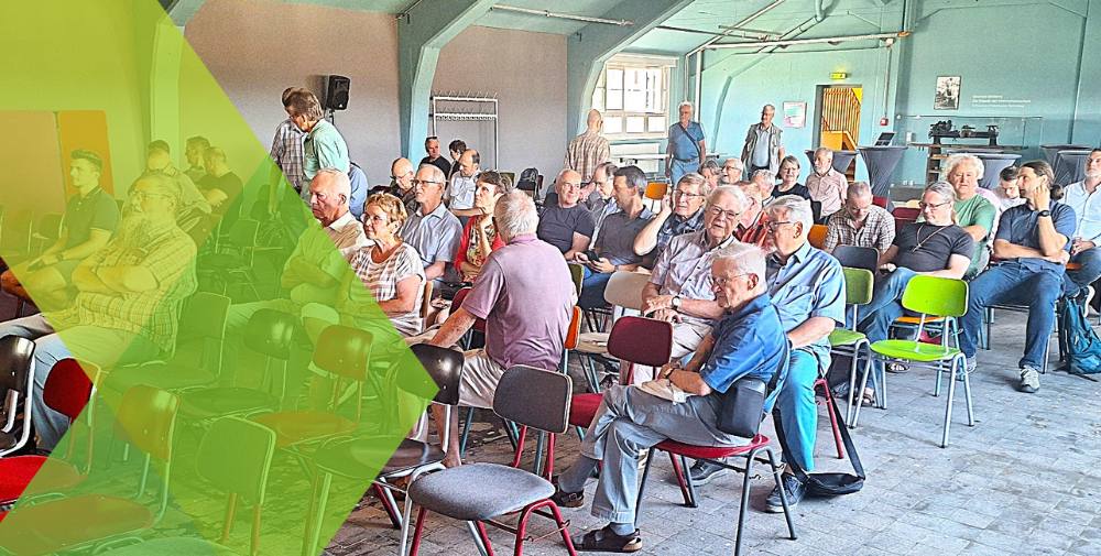
On June 23, 2026, a lecture was held at the Technische Sammlungen as part of the Microelectronics Alumni Series on the topic: “From UV to EUV—ZEISS’s Path to the World’s Leading Position in Lithography Optics.”
After a brief introduction and presentation of the speaker by curator Dr. Ralf Pulla, the lecture began.
Through the efforts of Dr. Reiner Pforr, Dr. Bernhard Kneer, Head of Product Systems Engineering at Carl Zeiss SMT GmbH in Oberkochen, delivered the lecture.
Short Biography of Dr. Bernhard Kneer
“Bernhard Kneer is the head of the Product Systems Engineering division at Carl Zeiss SMT GmbH in Oberkochen and is therefore responsible for the development of lithographic optical systems. After earning his Ph.D. in physics with a focus on quantum optics from the University of Ulm in 1999, he began his career at ZEISS in optical design. He then moved into systems engineering for optical systems. As Lead Systems Engineer, he led the development of the Starlith® 1700i optical system—the world’s first immersion lithography optic with a numerical aperture significantly greater than 1. He then led the development of high-NA EUV lithography optics, a crucial step for the latest generation of semiconductor manufacturing.
In 2006, Bernhard Kneer was awarded the German Innovation Prize as part of a team for the development of immersion optics. His work on the development of high-NA EUV lithography optics played a key role in ZEISS SMT being honored with the German Future Prize from the Federal President in 2020.”
After the first part provided a brief overview of the development of lithography systems from their inception—including a discussion of developments in the GDR by Carl Zeiss Jena—the second part was devoted to EUV systems.
EUV lithography represents the latest innovation in this field. It is already well established in the mass production of modern high-performance chips. Due to its short wavelength, it requires exclusively reflective optical elements that must operate entirely in a vacuum. This applies to the collector optics, the illumination system, and the projection lens. The limited reflectivity of the mirrors requires minimizing the number of optical elements and, consequently, fundamentally new system architectures compared to conventional DUV lithography.
With the so-called high-NA EUV lithography currently being introduced, resolution is being increased to approximately 8 nm. The increased numerical aperture requires optical systems with significantly larger geometries and larger mirrors, demands for their spatial positioning in the sub-nm range, and, as a result, extreme requirements for manufacturing and metrology. In parallel with the development of optical systems, a new industrial manufacturing infrastructure must be developed for this purpose, comprising the corresponding process equipment and metrology systems.
The presentation also explained the role of the Dutch company ASML as a major European equipment manufacturer that uses optical systems in its lithography equipment for the chip industry.
“ASML Holding N.V. (Advanced Semiconductor Materials Lithography) is a Dutch multinational company and the world’s largest supplier of lithography systems for the semiconductor industry. These highly complex machines play a crucial role in the manufacture of integrated circuits; most microchip manufacturers (foundries and IDMs) are ASML customers.” [Wikipedia]
ASML is the only provider of EUV technology worldwide.
It was a very interesting presentation that drew a crowd of about 70 people! Despite the very challenging topic, there was a lively discussion afterward with many questions.
Review
Inside Silicon Saxony
Long before the “Inside Silicon Saxony” event—scheduled for October 21, 2025—the 200 seats at the Dresden Technical Collections were sold out. No wonder. For the first time, top executives from Dresden’s five major semiconductor manufacturers—Infineon, esmc, Bosch, X-FAB, and GlobalFoundries—gathered here on one stage to share exciting insights into their fabs, their work, their products, target markets, and technologies.

Cooperation desired
Were you previously involved in the microelectronics industry in Saxony, or do you know someone who was?
Then please feel free to contact us!
YOUR CONTACTS

Susann Irrgang
+49 351 8503-2923
susann.irrgang@silicon-saxony.de

Thomas Haase
+49 351 4128-051
THAASEDD@t-online.de

