
Company type
Home | Mitglieder |
Onto Innovation Germany GmbH
Medium-sized companies (<250 employees or <50 million annual turnover)
Target markets
Electronics
Industries
Production·Software
Portfolio
Advanced Packaging Lithography·Electronic·Equipment·Equipment Control Software·Micro- / Nanoelektronics·Process Control Software·Semiconductor Industry·Software·Thin Film Metrology·Yield Management Software
Certificates

Contact
Antonstraße 39
01097 Dresden
01097 Dresden
+1 978.253.6200
Contact Person
Dr. Dirk Bisping
About this member
Onto Innovation is a leader in process control, combining global scale with an expanded portfolio of leading-edge technologies that include:
- Un-patterned wafer quality
- 3D metrology spanning chip features from nanometer scale transistors to large die interconnects
- Macro defect inspection of wafers and packages
- Metal interconnect composition
- Factory analytics
- and lithography for Advanced Semiconductor Packaging.
Our breadth of offerings across the entire semiconductor value chain combined with our connected thinking approach results in a unique perspective to help solve our customers most difficult yield, device performance, quality, and reliability issues.
Onto Innovation strives to optimize customers critical path of progress by making them smarter, faster and more efficient.
Headquartered in Wilmington, Massachusetts, Onto Innovation supports customers with a worldwide sales and service organization.
Additional information can be found at www.ontoinnovation.com
Overview
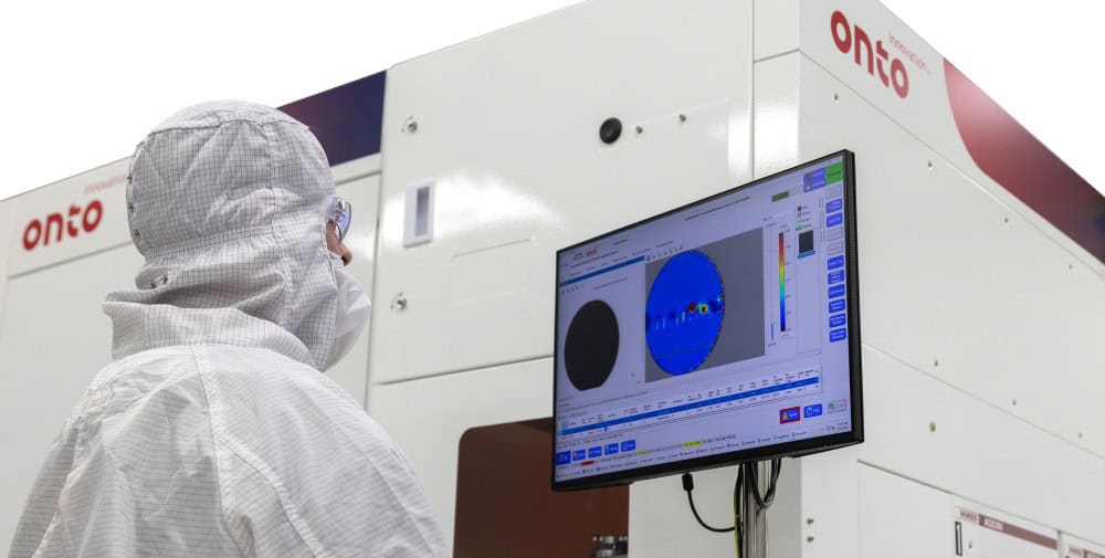
Onto Innovation is a leader in the design, development, manufacture and support of defect inspection, advanced packaging lithography, process control metrology, and data analysis systems and software used by semiconductor device manufacturers worldwide.
Onto Innovation provides a full-fab solution through its families of proprietary products that provide critical yield-enhancing information, enabling microelectronic device manufacturers to drive down the costs and time to market of their products.
The Company’s expanding portfolio of equipment and software solutions is used in both the wafer processing and final manufacturing of ICs, and in adjacent markets such as FPD, LED and Solar.
Areas
Inspection Equipment, Measurement Equipment, Defect Inspection, Particle, Bump, Advanced Packaging Metrology and Inspection, Contamination Detection, Review, Die Inspection, Film Thickness, Uniformity Measurement, Ellipsometer, Metal Film Thickness, All Surface Inspection, Factory Monitoring and Control System, Automatic Defect Classification, Process Control, Production Control Software, Yield Management

