Company type
Home | Mitglieder |
KMLT GmbH
Small companies (<50 employees or <10 million annual turnover)
Target markets
Electronics·Machinery and Equipment·Public Sector
Industries
Production·Technology·Technology Users·Upstream Industry
Portfolio
·Calibration Masks·Calibration Templates·Cleanroom-Compatible Labels·DMC Labels·Electro Polishing·High Precision Stencils·Laser Engraving·Laser Fine Cutting·Laser Marking·Laser Micro Cutting·Laser Micro Processing·Laser Micro Structuring·Masks for OLED·Micro Bending·Micro Polishing·SMD Stencils·Tamper-Proof Labels
Certificates
Contact
Freiberger Str. 114
01159 Dresden
01159 Dresden
0351 / 41666-0
Contact Person
Dipl.-Ing. Kalman Kirchner
0351 41666 0
Geschäftsführer
About this member
KMLT® is your specialist for laser micro-machining and laser material processing for products with high precision requirements down to the single-digit µm range.
With the founding of KIRCHNER UND MÜLLER LASERTECHNIK GbR in Dresden in the spring of 1991, one of the first laser job shops in eastern Germany was established.
In the early years, KMLT® focused exclusively on laser contract marking. With increasing acceptance, growing sales, and the goal of tapping into larger markets, the company was converted into a limited liability company (GmbH) in 1993.
The goal of exploring further areas of application for laser technology led to the founding of the subsidiary DREMICUT GMBH in 2001. Since then, the production site in Neukirch/Lausitz has focused on laser micro-machining, laser micro-cutting, the manufacture of SMD precision stencils, and laser micro-welding.
At the end of 2020, KIRCHNER UND MÜLLER LASERTECHNIK GMBH was renamed KMLT GmbH. In 2021, both companies were merged to form KMLT GmbH. Today, a wide range of 26 laser systems forms the technical foundation for the implementation of versatile and demanding applications.
Our special machines are perfect for manufacturing precision parts from almost all metals, precious metals and alloys in material thicknesses from 0.005 mm to 3.0 mm. We offer various processes for different accuracy ranges.
In order to keep pace with this successful development, an additional warehouse was built, which was completed in August 2025. This created space for new laser systems—including an UKP femtosecond laser and other machines—at the Neukirch site.
Detail of a stencil for wafer bumping (75µm thickness)
The application of the relevant amounts of solder for the components is implemented primarily through the correct selection of the required stencil thickness. This selection is influenced by the basic design rules applicable to the components. A final decision, however, is always in the hands of experienced manufacturing engineers.
Normally, different volumes of the paste can be applied due to the professional design adjustments of the pad structure.
Alternatively stepped stencils can be used. In this case the required solder paste volumes are regulated by partial adjustment of the stencil thickness.
Precision stencils for wafer bumping, BGA, LTCC, Solar
Precision plates above 50µm thick are used for wafer bump stencils. These are processed tension free and to high accuracy in climate controlled conditions with highly accurate laser systems.
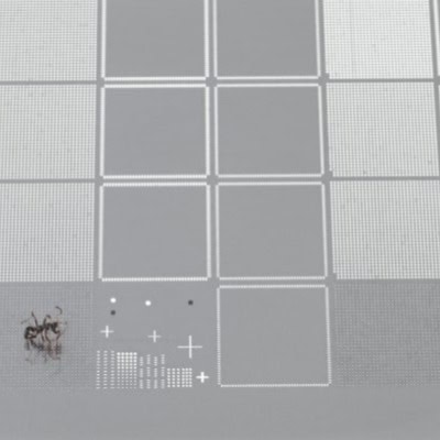
Wafer Bump Stencil - KMLT®
SMD stencils, high precision stencils, calibration stencils, masks
Laser micro cutting, SMD stencils, laser marking, laser engraving: since 1991 KMLT® has been the specialist for reliable contract manufacturing in the demanding field of precise laser micro processing.
We cut precision parts from a variety of conceivable metals, precious metals and alloys from a material thickness of 0.005 mm to 3.0 mm.
Our specialization enables cuts with low burr formation and highest accuracy. Depending on the part geometry and material properties, manufacturing tolerances of up to ±3 µm are feasible and can be verified by protocol.
We manufacture parts for mechanical watches, spring elements, shielding plates, masks, SMD stencils, fitting rings and precision tube parts of all kinds, both as individual parts and in series.
The range of services and scope of delivery in the field of precision stencils includes:
– Laser micro cutting of SMD metal stencils from special stencil sheet (stainless steel, nickel) up to a thickness of 600 µm
– Metal stencils for adhesive application
– Placement and placement control stencils
– Stencils for wafer bumping
– Special stencils for LTCC, BGA, FinePitch applications
– Printing stencils for solar technology – Special stencils with material thicknesses from 5 µm
– Masks for OLED technology and others
– License-free perforations for all common quick clamping systems
– Machine brushing for optimal doctoring processes
– Electropolishing
– Nano-coating
– Edge protection – protection against cuts
– Quick-change frames of various ZelFlex types or VectorGuard®
– Preparation of a quality report
– Provision of data for 3D paste inspection
– EXPRESS service with same-day delivery
Further information at: www.kmlt.de
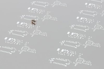
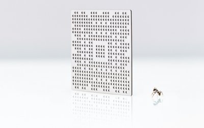
SMD stencil
Stencil for BGA/µBGA
These place particularly high demands on the laser equipment and the engineer’s technical know-how.
It is dependent here upon placing the least thermal demand on the material. The results are deformation free stencils with up to several hundred thousand pads.
Special demands on the stencil production need to be considered for semiconductor and hybrid technologies.
By using these precision stencils different substances can be applied in print procedures.
Stencil for solder paste printing for a BGA component
In the case of printing using BGA/μBGA, LTCC, Solar, flip chip technologies and for particular high density stencils, metal foils are used with a material thickness from 20 μm.
The production of these stencils, tension free, plane and with very high accuracy, places particularly high demands on our production technology and know-how.
As is true for the wafer bump stencils, the material must be minimally thermally affected in order to produce deformation free stencils with sometimes more than one hundred thousand openings.
Find more information: www.kmlt.de
BGA Stencil - KMLT®