Strong cooperation for tomorrow’s semiconductor manufacturing technologies
The signed Strategic Partnership Agreement extends the strategic partnership between imec and ZEISS, which has already existed since 2019, until 2029. “We are very pleased to intensify our cooperation with imec in order to further advance tomorrow’s semiconductor technologies together with its strong partner network,” explains Thomas Stammler, Chief Technology Officer and member of the management of ZEISS SMT. Since 1997, imec and the ZEISS Semiconductor Manufacturing Technology division have been working on various joint projects to continue Moore’s Law, which is used to continuously increase the performance of microchips and memory processors. “The expertise and technological experience of industrial partners such as ZEISS are essential for the research and further development of state-of-the-art semiconductor technologies. We are therefore very pleased to put our partnership on an even stronger footing,” says Luc Van den hove, President and Chief Executive Officer of imec.
With the signed agreement, the two cooperation partners are reaffirming their joint efforts to further develop key semiconductor manufacturing technologies such as high-NA-EUV lithography. In the future, it will enable the production of even more powerful and energy-efficient microchips, which are the basis for key technologies such as artificial intelligence, autonomous driving, Industry 4.0 or pioneering solutions for medical technology and the energy transition.
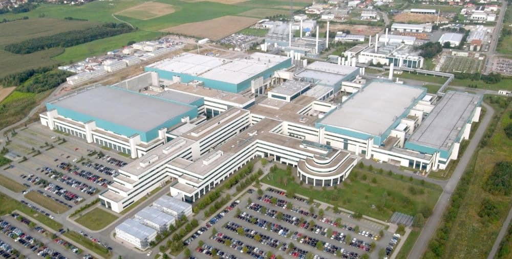
Imec’s pilot line as a research center for the global semiconductor industry
ZEISS supports imec as part of the agreement not only by participating in research projects for the further development of manufacturing, process and measurement technologies for semiconductor production. The provision of lithography optics of various product generations for imec’s pilot line, which are integrated into the lithography scanner systems of the strategic partner ASML, are also an essential part of the cooperation.
Imec’s pilot line, which is now being expanded with the NanoIC pilot line and is operated in Leuven, Belgium, covers the entire value creation process as well as various technology strands for semiconductor manufacturing. It aims to give industry representatives such as end customers, suppliers and research institutions access to pioneering and currently most advanced semiconductor technologies and platforms with which they can research, develop and test innovations. It will also drive the optimization of existing equipment, processes and measurement methods to enable ever smaller, more powerful and more energy-efficient microchips and thus advance global digitalization. The collaboration will be deepened through ZEISS’ participation in various industry partner programs, such as Advanced Patterning, 3D System Integration and Optical Interconnect, under the leadership of imec. The programs will work together on the latest process and inspection techniques for process optimization of next-generation semiconductors.
Investments in line with the European Chips Act
The close collaboration between imec and ZEISS is in line with the goals and ambitions of the European Union and the European Chips Act, which aims to strengthen Europe’s technological sovereignty, competitiveness and resilience. “With the investments in imec’s pilot line, which is now being expanded with the NanoIC pilot line, ZEISS is making a significant contribution to maintaining Europe’s lead in the latest generation of semiconductor equipment and further expanding it through the further development of technology roadmaps,” says Stammler. The strengthened cooperation between the two partners also sends a signal about the relevance of cross-industry networking for the global semiconductor market: “This strategic partnership between imec and ZEISS underlines how strong cohesion among European partners accelerates innovation and strengthens Europe’s leadership position in the semiconductor ecosystem – and is crucial for building the NanoIC pilot line, the world’s most advanced infrastructure for research and development in the field of technology nodes below two nanometers,” says Van den hove.
The acquisition and operation of the NanoIC pilot line is jointly funded by Chips Joint Undertaking, European Union’s Digital Europe (101183266) and Horizon Europe programs (101183277), as well as by the participating countries Belgium (Flanders), France, Germany, Finland, Ireland and Romania. For more information, visit www.nanoic-project.eu.
– – – – – –
Further links
👉 www.zeiss.de
Photo: ZEISS