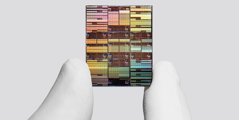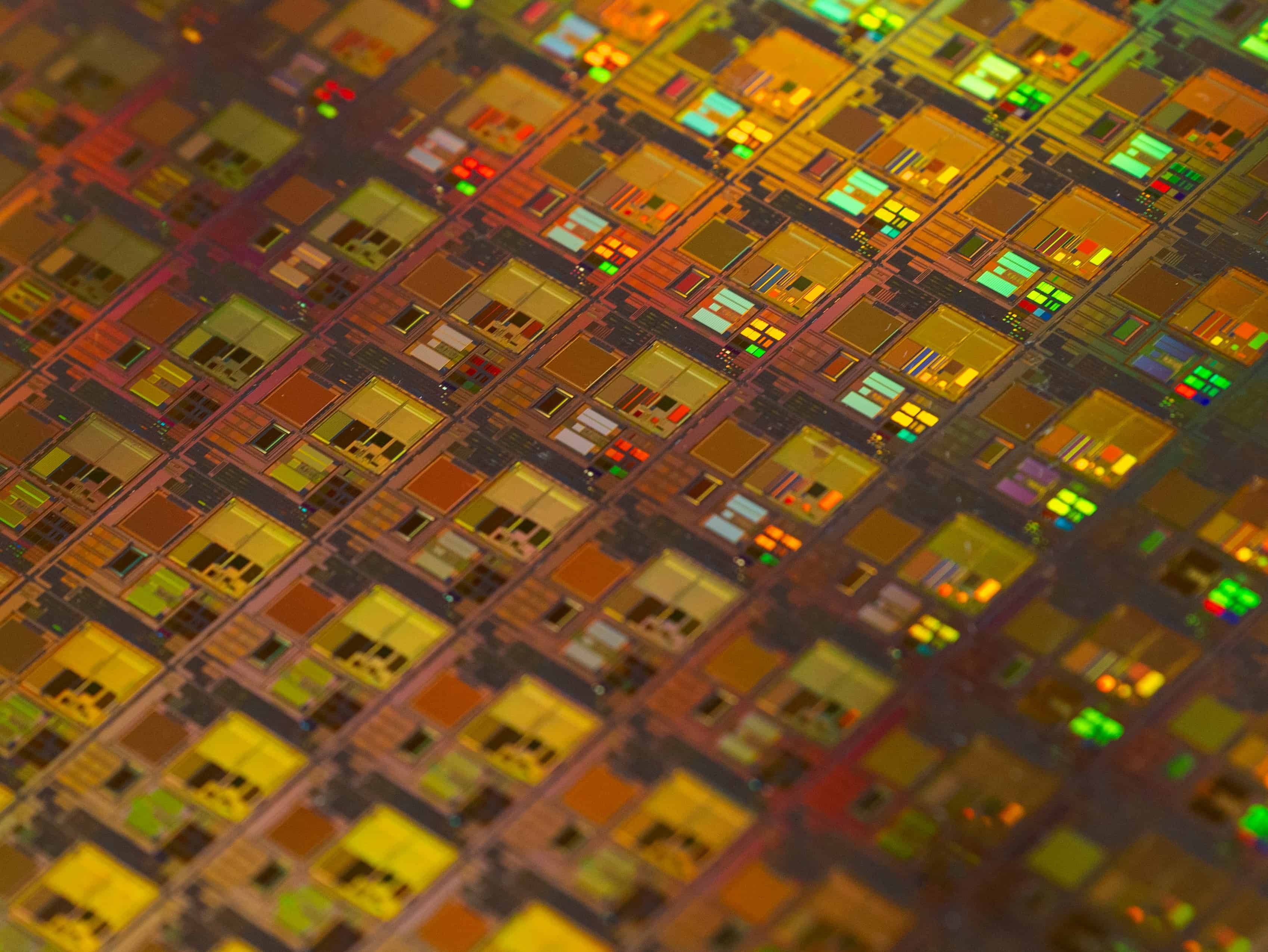
IBM’s new sub-1-nm chip integrates nearly 100 billion transistors on an area the size of a fingernail—almost twice the density of the 2-nm chip IBM unveiled in 2021. This is made possible by a series of structural and materials-related innovations, including IBM’s groundbreaking three-dimensional nanostack architecture. This demonstrates that performance and efficiency gains are still possible, even as chip structures approach features on the atomic scale.
Published technical results show that the new chip is expected to enable a significant performance leap—up to 50 percent more performance or 70 percent higher energy efficiency compared to IBM’s 2-nm chips [1] —thereby massively accelerating applications ranging from generative AI to cloud infrastructure and future electronic devices.
“IBM’s latest breakthrough in chip technology marks a turning point in computing and shifts the technology from the nanometer era to the atomic scale. With our new Nanostack architecture, we’re not just shrinking transistors—we’re fundamentally redefining how chips are built to achieve significantly greater performance and energy efficiency,” said Jay Gambetta, Director of IBM Research and IBM Fellow. “This industry-first innovation continues IBM’s leadership in future technologies and lays the foundation for the next era of computing.”
Nanostack – Breakthrough in Chip Design
To manufacture this chip, IBM researchers developed a completely new transistor architecture called “Nanostack”—the industry’s first known three-dimensional, nanosheet-based design. Nanostack represents a significant advancement over nanosheet technology, the industry’s current leading architecture, which was also developed by IBM. The Nanostack design stacks and offsets transistors vertically and uses 3D sequential integration to fit more transistors onto a single chip. Furthermore, it allows for the use of different material combinations in each layer, enabling the performance and energy efficiency of each transistor to be optimized independently.
IBM’s nanostack architecture has been experimentally validated—including through ultra-thin dielectric bonding in CMOS integration, demonstrations of dual-channel engineering, and functional CMOS inverters that exhibit the expected switching performance. These results confirm that nanostack technology is practically feasible and supports real computing functions.
In addition, IBM researchers demonstrated at VLSI 2026 that the nanostack architecture enables a 40 percent scaling for SRAM [2], thereby enabling chip designers to develop significantly more efficient chips while meeting the high-bandwidth requirements of advanced AI workloads.
With this groundbreaking structure, semiconductor structures can be developed below the 1-nm threshold for the first time. This brings scaling into the angstrom range, where dimensions approach the size of individual atoms. Although technology nodes today refer more to a generation of manufacturing technology than to an exact physical dimension, IBM’s 0.7-nm technology—also known as 7 angstroms—demonstrates how further scaling is possible. With the new nanostack architecture, IBM’s semiconductor roadmap promises at least another decade of scaling potential.
Decades of Leadership in Semiconductor Innovation
This breakthrough underscores IBM’s role as a leader in semiconductor research and development. For decades, IBM has driven the global development of chips that power computer systems—from early semiconductors in the 1960s to the world’s first 2-nm chip. IBM continues to innovate in cutting-edge silicon technology, AI hardware, logic, and quantum processors to enable the future of computing.
IBM and its partners are conducting this work at a renowned semiconductor research facility in Albany, New York. This facility will soon house a high-numerical-aperture (High NA EUV) extreme ultraviolet lithography system—essential for the future scaling of semiconductor technology nodes. This technology, developed by ASML, enables high-precision circuit fabrication and supports the production of smaller, more powerful chips. IBM and its partners—including Lam Research Corp. (Nasdaq: LRCX), Tokyo Electron (TEL), and SCREEN Semiconductor Solutions, Ltd.—have collaborated on new High NA EUV processes and tools that have already produced functional devices.
IBM also recently announced plans to establish Anderon, the world’s first dedicated foundry for quantum chips. Anderon, an independent IBM company, will draw on IBM’s industry-leading expertise in quantum computing and semiconductors to enable the United States to produce a significant portion of the world’s quantum wafers.
With the expectation of an early introduction of nanostack technology in the sub-1 nm range, IBM sees a path to production readiness within the next five years.
About IBM
IBM is a leading provider of global hybrid cloud and AI, as well as consulting services. We help clients in more than 175 countries leverage insights from their data, optimize business processes, reduce costs, and gain a competitive edge. Thousands of governments and companies in critical infrastructure sectors such as financial services, telecommunications, and healthcare rely on IBM’s hybrid cloud platform and Red Hat OpenShift to drive their digital transformation quickly, efficiently, and securely. IBM’s groundbreaking innovations in AI, quantum computing, industry-specific cloud solutions, and consulting provide our clients with open and flexible options. All of this is based on IBM’s longstanding commitment to trust, transparency, responsibility, inclusion, and service. For more information, visit www.ibm.com.
———————-
[1] S. Reboh et al., “NanoStack Transistor Architecture for CMOS 7A Node and Beyond,” VLSI 2025
[2] Chen Zhang et al., “Area and Performance of Staggered-Channel Nanostack SRAM Bitcells,” VLSI 2026
– – – – –
Related Links
👉 www.ibm.com
Photo: IBM