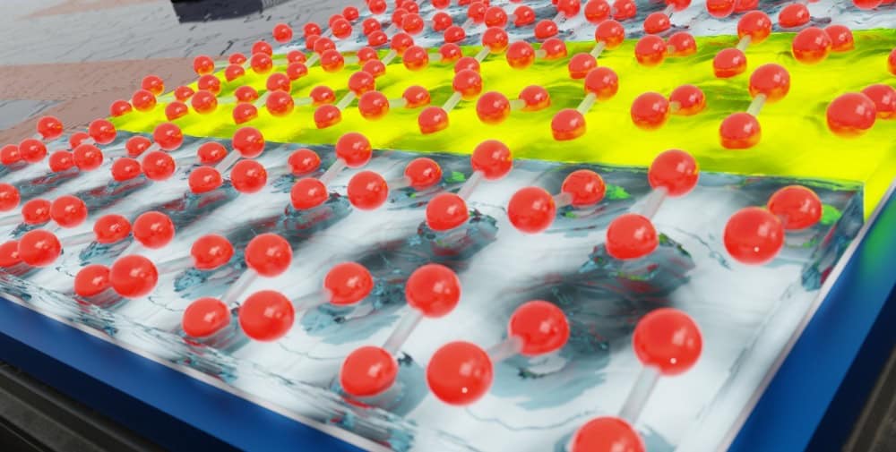
At low temperatures, pairs of silicon atoms form on a silicon surface, so-called dimers, which can tilt either to the right or to the left like a seesaw. Above a critical temperature – in the case of silicon, this is 190 Kelvin (-83 °C) – the dimers wobble back and forth between the two states. “When cooling below the critical temperature, the dimers lock into one of the two states,” says Dr. Gernot Schaller, Head of Quantum Information Technology at the Institute of Theoretical Physics at the HZDR. “They are virtually frozen during this phase transition.”
In addition, the individual dimers influence each other. However, this influence depends on the arrangement of the dimers: The coupling in the transverse direction is stronger than in the longitudinal direction. “And it is precisely this strong, so-called anisotropy that is essentially responsible for the behavior of the silicon dimers on the surface,” says Schaller. “Depending on the cooling rate, we see a transition from one-dimensional to two-dimensional behavior.” One-dimensional means that extremely rapid cooling by more than 100 degrees per microsecond causes the tilt angles of the dimers to adjust along long chains. If, on the other hand, the temperature drops more slowly, the two-dimensional behavior dominates. In this case, the silicon dimers form more or less large, ordered surfaces, so-called domains, which are characterized by a uniform honeycomb structure. “And the slower the cooling process, the larger these domains become,” explains Schaller.
The researchers used the Ising model to calculate the crystalline surface structure. This mathematical model considers the tilt angles of the silicon dimers, which can only assume one of two possible states. Thanks to the anisotropic Ising model, this elegant description of a phase transition during the shock freezing of silicon surfaces is not just gray theory. The researchers also compared their analytical and numerical calculations with experimental data.
Honeycombs and zigzag chains
High-resolution images from a scanning tunneling microscope of deep-frozen silicon surfaces show structures that are consistent with the simulations. Both extended two-dimensional honeycomb structures and sharp one-dimensional boundaries between zigzag chains can be clearly seen. “And our colleagues from the University of Duisburg-Essen have planned further experiments that could prove the influence of the cooling rate on the structure of the silicon surface – in a way that is completely analogous to our simulations,” says Prof. Ralf Schützhold, Director of the Institute of Theoretical Physics at the HZDR.
However, the results not only provide new impetus for the targeted production of defect-free silicon surfaces. “The behavior of the silicon dimers also shows parallels to the so-called Kibble-Zurek mechanism,” says Schützhold. Named after the theoretical physicists Tom Kibble and Wojciech Hubert Zurek, this theoretical model describes how topological defects, i.e. defects in an ordered structure, arise when a phase transition occurs quickly. Kibble looked at processes during the cooling of the very young universe after the Big Bang. Topological defects, such as point-like monopoles or linear defects – the cosmic strings – could have arisen in the process. Zurek predicted an analogous behavior in condensed matter using the example of cryogenic, superfluid helium. And now the team led by Schaller and Schützhold has proven that the Kibble-Zurek mechanism is apparently even more widespread than previously assumed and can even occur in shock-frozen silicon surfaces.
Contact
Simon Schmitt | Head and Press Spokesperson
Department of Communication and Media at the HZDR
Tel.: +49 351 260 3400 | E-Mail: s.schmitt@hzdr.de
Further links
👉 https://www.hzdr.de
Photo: B. Schröder/HZDR