Integrated photonic systems combine electronics, active and passive optical components, and other technologies. For example, light emitters (e.g., lasers, organic light-emitting diodes/OLEDs, microLEDs), waveguides, modulators (e.g., area light modulators or microscanner mirrors), and detectors can be combined to form powerful, complex systems. The integration of various functions into a small space enables compact and potentially energy-efficient solutions for a wide range of applications.
“Integrated photonics opens up new possibilities for combining optical and electronic functions in compact systems,” explains Prof. Dr. Wenke Weinreich, Director of the Fraunhofer IPMS. “With our expertise in development and manufacturing, we aim to help make these technologies usable for new applications. It is crucial to consider the entire development chain, from the technology to the integrated system.”
Wide Range of Applications and Research Topics
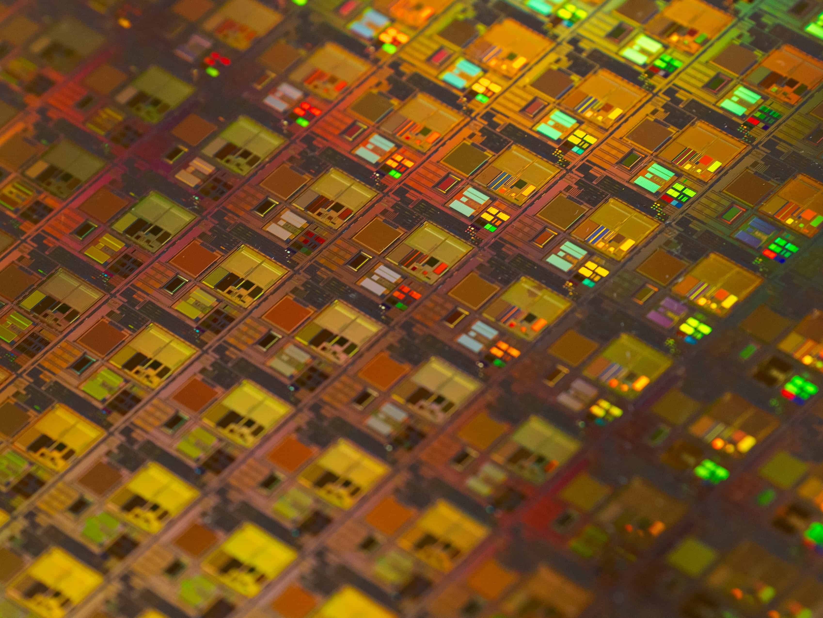
A key focus of Fraunhofer IPMS in the field of integrated photonics is the development of electro-optical components and associated CMOS-compatible fabrication technologies on 200- and 300-millimeter wafers. A central technological foundation for this is the silicon nitride (SiN) waveguide platform, which is available for both wafer sizes. It is characterized by very low optical losses across a broad wavelength spectrum ranging from the visible to the mid-infrared range, thereby enabling the realization of complex photonic circuits. This platform not only serves as the foundation for highly sensitive photonic biosensors but also forms the backbone for many other applications. These include, among others, photonic computing, quantum technologies, and hybrid integration with active components. Electronic and optical functionalities are integrated at the wafer level, allowing the resulting devices to be manufactured cost-effectively in large quantities.
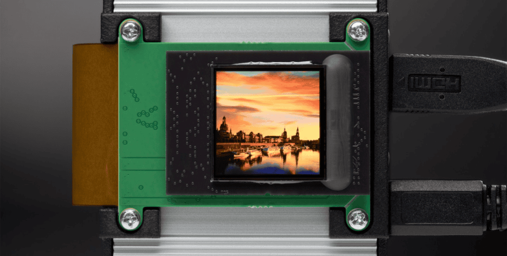
The Fraunhofer IPMS’s research portfolio encompasses a wide range of innovative technologies. These include area light modulators based on MEMS (microelectromechanical systems) technology, featuring millions of analog-controlled micromirrors that are individually driven by integrated CMOS electronics. They enable highly precise spatial and temporal light modulation for a wide range of applications and are used, for example, in mask-less microlithography, optical quantum computing, and holography. In addition, Fraunhofer IPMS is developing high-resolution OLED microdisplays with resolutions currently up to 2,048 x 2,048 pixels. They combine a CMOS backplane for individual pixel control with OLED materials for light generation and are particularly suitable for smart glasses and other compact display systems.
Developing new solutions together with industry partners
To further develop integrated photonic systems, Fraunhofer IPMS is systematically expanding its technological expertise and manufacturing capabilities. The focus is on concrete new integration approaches, such as the monolithic and hybrid combination of the SiN waveguide platform with active components like micro-scanner mirrors or lasers, as well as the scaling of 300-mm manufacturing. Through close collaboration with industry partners, the institute carries out customer-specific pilot manufacturing and directly adapts technological developments to specific product requirements, such as for use in medical technology, the automotive sector, or quantum systems.
To bring together stakeholders from research and industry and to promote the exchange of ideas on new technological developments and applications, Fraunhofer IPMS organized the Industry Partner Day on August 20, 2026. Under the title “Photonics for Next-Generation Information Systems,” participants discussed current developments and future prospects in integrated photonics.
“The exchange with our industry partners is a key component in aligning technological developments with the requirements of future markets at an early stage and jointly developing new solutions,” Weinreich concluded.
– – – – –
Related Links
👉 www.ipms.fraunhofer.de
Photo: Fraunhofer IPMS