Numerous applications benefit from the image quality and high brightness of OLED microdisplays. For example, these displays are used in augmented reality (AR) glasses for vivid and clearly visible content under very different lighting conditions or in virtual reality (VR) headsets for realistic and bright images. They are also used in military applications for clear visibility of commands and location cues in military devices under extreme conditions.
OLEDs are considered limited in very high brightness in harsh environments. This is why microLEDs are often advertised as an alternative, which are said to achieve brightness levels (luminance) even in the region of one million cd/m². However, microLEDs have a significant loss of efficiency at very high pixel densities, as required in high-resolution microdisplays. This means that they have to be operated at more than 1A/cm². In addition, this technology is not yet mature, especially for full color. In contrast, the current density for OLEDs in long life cycle operation is typically less than 100 mA/cm².
However, these limitations can be greatly improved by stacking multiple OLED layers on top of each other. However, the current density of the individual OLED layers is limited to ensure adequate lifetime and reliability. However, stacking OLED layers increases the voltage drop and swing across the OLED stack. Now, a high-voltage CMOS backplane for high-brightness OLED microdisplays has been developed.
Dr. Uwe Vogel, Head of “Microdisplays and Sensors” at Fraunhofer IPMS, explains: “We have developed an innovative pixel cell design that enables a voltage swing of over 10 volts and is thus capable of driving multiple stacked, upward emitting OLED layers. Depending on the number of stacked units, multiples of maximum emission can be achieved with high current efficiency while maintaining constant current density. This approach enables full color maximum brightness of over 10,000 cd/m² while maintaining lifetime and reliability.”
The advantages of OLEDs over microLEDs are striking:
- Mature technology: OLED technology has reached a high level of maturity and there are already many established products on the market. MicroLEDs are not yet as advanced, especially for displaying full color.
- Lower current density: OLEDs can operate at a current density of <100 mA/cm² in typical operation, which gives them higher efficiency and longer life. MicroLEDs, on the other hand, often require more than 1A/cm², which leads to a significant loss of efficiency.
- Brightness increase through stacking: The ability to stack multiple OLED layers on top of each other can increase brightness to more than 10,000 cd/m². This improves the application possibilities in bright environments.
In summary, OLEDs are advantageous in many applications due to their maturity, efficiency and color display, while microLEDs still need work on the technology to offer similar benefits.
Through the application of multi-stacked OLEDs on a high-voltage CMOS backplane, this brightness can now be extended to about 10,000 nits, which significantly increases the market opportunities for very bright OLED microdisplays.
Fraunhofer IPMS has been developing backplanes for various technologies and especially microdisplays for many years. The institute has developed a globally unique development know-how that covers the entire process chain from the feasibility study to pilot production (for OLED microdisplays). The scientists are looking forward to bringing the new backplane technology to market with industrial partners.
– – – – – –
Further links
👉 www.ipms.fraunhofer.de
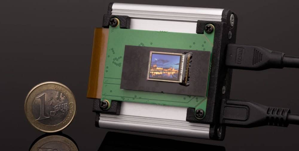
Photo: Fraunhofer IPMS