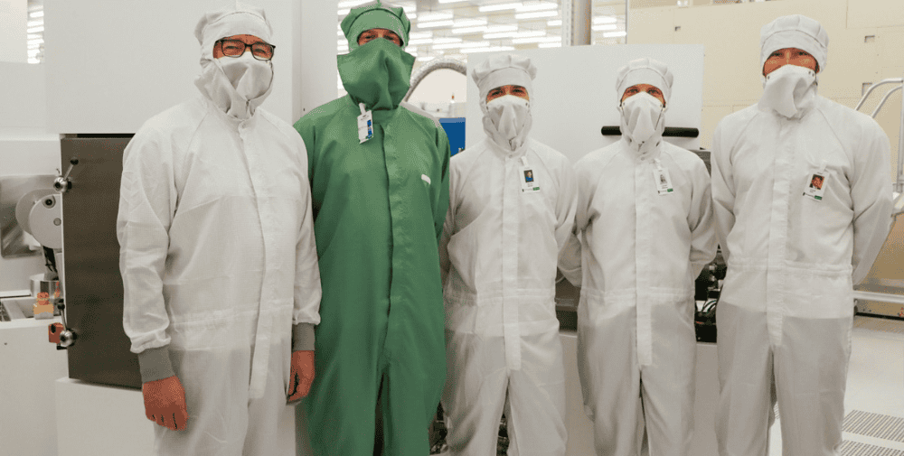
The system represents an important step in Fraunhofer IPMS’s strategy to bridge the gap between basic research in materials science and industrial semiconductor manufacturing. “Scalable quantum computing requires manufacturing technologies that combine outstanding material quality with semiconductor-compatible production processes,” says Prof. Dr. Wenke Weinreich, Director of Fraunhofer IPMS. “With this new PVD platform, we are expanding our capabilities to develop and qualify superconducting materials under CMOS-compatible conditions and to accelerate their transfer to industrial manufacturing. This is an important milestone for us in establishing a European quantum research factory.”
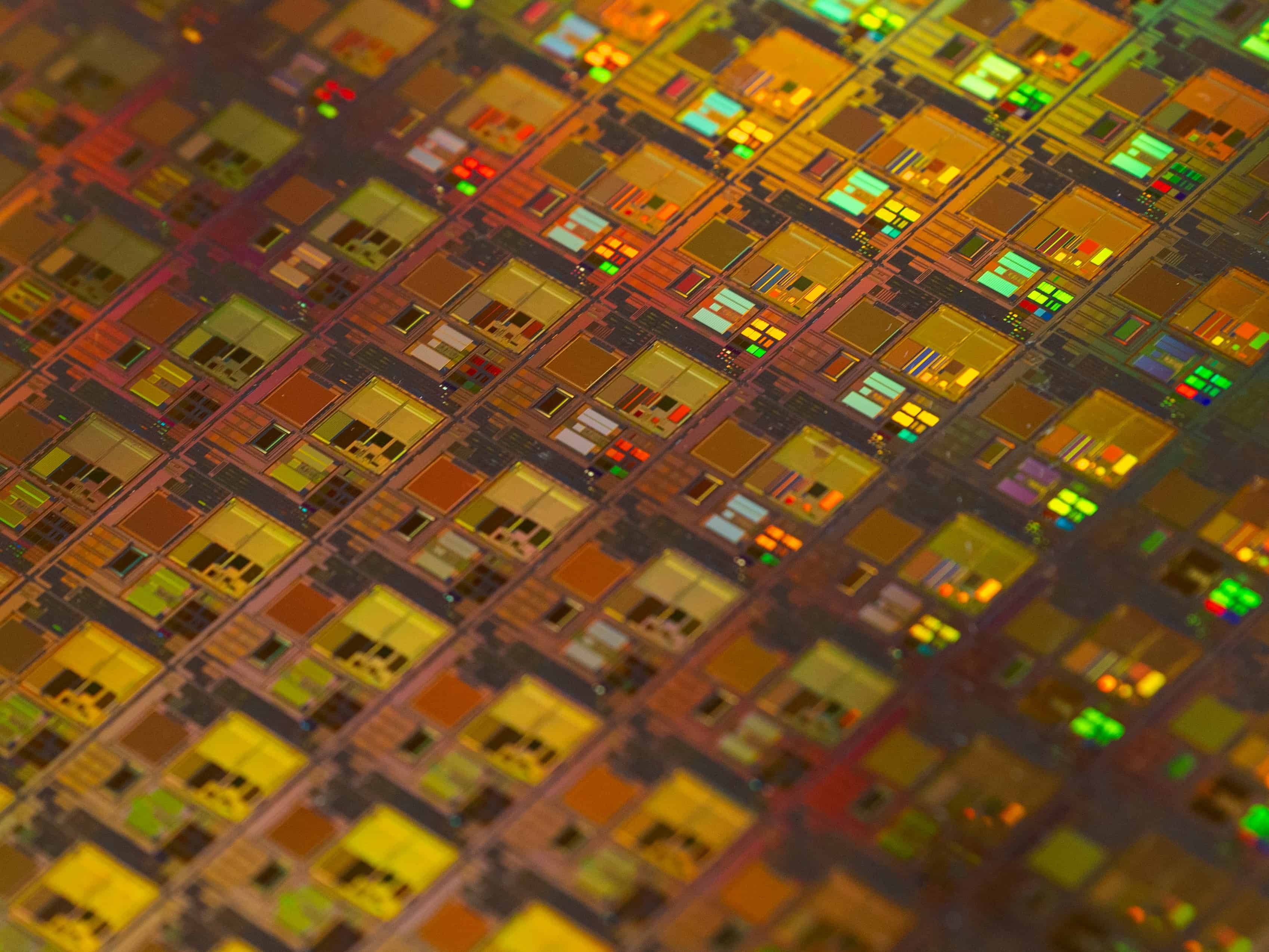
Polyteknik’s Flextura PVD system integrates multiple deposition technologies and enables researchers to develop complex material stacks consisting of metals, nitrides, and oxides. These material combinations form the basis for superconducting circuits and other key components needed for future quantum processors. Initial process developments have already shown promising superconducting properties for niobium nitride (NbN) and zirconium nitride (ZrN), which were deposited directly onto 300-mm wafers. These materials, some of which were demonstrated for the first time by Fraunhofer IPMS, hold enormous potential, according to Weinreich: “Our results show material properties that are consistent with the values reported in the scientific literature, thereby demonstrating the platform’s ability to develop high-performance quantum materials on an industrial 300-mm wafer format. We achieve these reference properties at higher deposition rates and with excellent layer uniformity, while the system’s flexibility allows us to continuously refine these processes.”
The new platform is fully integrated into the Fraunhofer IPMS 300-mm cleanroom environment and complements the institute’s process portfolio within the framework of the German Microelectronics Research Factory (FMD). It also supports several major European pilot line initiatives, such as APECS, SUPREME, and SPINS, which aim to strengthen the European ecosystem for semiconductor and quantum technology.
Beyond research activities, the expanded infrastructure offers industry partners direct access to a state-of-the-art 300-mm R&D environment for process validation, material qualification, and technology development. This enables companies to evaluate innovative materials and device concepts under manufacturing conditions that closely resemble future mass production.
Funding Note:
The tool was procured as part of the SMWK project “3D4QC,” which is co-funded by the Free State of Saxony and the European Union.
About Fraunhofer IPMS
Fraunhofer IPMS is a leading international research and development service provider for electronic and photonic microsystems. Our technologies find applications in industry, mobility, biotechnology, and medical technology. At the same time, we address key future fields such as quantum technologies and neuromorphic computing. Through our research in the field of green microelectronics, we contribute to a resource-efficient and sustainable world. Through the Center Nanoelectronic Technologies (CNT), Fraunhofer IPMS offers applied research on 300-mm wafers for microchip manufacturers, suppliers, device manufacturers, and R&D partners.
– – – – –
Related Links
👉 www.ipms.fraunhofer.de
Photo: Fraunhofer IPMS