July 24, 2024. German research partners demonstrate for the first time the practical implementation of an aluminum nitride-based value chain for power semiconductors, from base material to device manufacturing.
Categories
July 24, 2024. German research partners demonstrate for the first time the practical implementation of an aluminum nitride-based value chain for power semiconductors, from base material to device manufacturing.

Categories
Tags
Contact info
Silicon Saxony
Marketing, Kommunikation und Öffentlichkeitsarbeit
Manfred-von-Ardenne-Ring 20 F
Fax: +49 351 8925 889
Contact person:

A new semiconductor technology based on aluminum nitride (AlN) for power electronic transistors and millimeter wave radio frequency circuits has the potential to significantly reduce losses in the conversion of electrical energy and in radio frequency transmission. At present, established silicon components in power electronics are being replaced by more powerful semiconductors with a large band gap (WBG), i.e. with better physical and electrical properties. Silicon carbide (SiC) has already established itself on an industrial scale, but components made of gallium nitride (GaN) are also on the rise. However, it is already foreseeable today that even WBG components will be surpassed in their properties by semiconductors with an ultra-wide band gap (UWBG) in the future. One promising UWBG semiconductor is AlN. Components on single-crystal AlN wafers achieve a higher stable power density and efficiency compared to GaN technology. They also exhibit lower dynamic interference effects and greater reliability. At the same time, the high thermal conductivity of AlN enables good heat dissipation of the components.
In order to make AlN technology accessible to industry in the medium term, the existing activities on this material in Germany have been bundled in a strategic cluster. The aim is to establish a German value chain for AlN-based technology and to build up an international leadership position in this increasingly economically important field. The Ferdinand-Braun-Institut, Leibniz-Institut für Höchstfrequenztechnik (FBH), the Fraunhofer Institute for Integrated Systems and Device Technology IISB and the company III/V-Reclaim PT GmbH are jointly driving these activities forward. They cover the entire value chain, starting with the growth of AlN crystals using the physical vapor transport (PVT) process, wafering and polishing of epitaxial AlN wafers and the epitaxy of functional device layers through to the production of transistors for power electronics and millimeter wave applications.
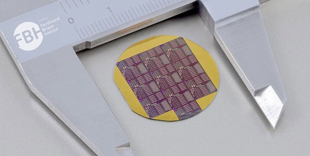
The consortium has succeeded in successfully demonstrating the practical implementation of the value chain for AlN devices for the first time in Germany and Europe. To this end, AlN crystals were grown at Fraunhofer IISB and sawn into AlN wafers with a diameter of up to 1.5 inches. The company III/V-Reclaim has developed a polishing process for the production of epitaxial wafers. Functional epitaxial layers were applied to these wafers at the FBH and AlN/GaN transistors with high electron mobility (HEMTs) were successfully processed on them. The first transistor generations produced in this way show promising electrical properties, such as a breakdown voltage of up to 2200 V and a power density that exceeds that of components made of SiC and GaN.
The pursuit of ever greater energy efficiency and progressive miniaturization is also crucial for power electronic systems and in microwave communication. However, the static and dynamic conduction losses in the semiconductor materials unnecessarily increase the switching losses in the provision, distribution and use of electrical energy and therefore the consumption of valuable primary energy. In Europe, for example, an estimated 3 terawatt hours of electrical energy are wasted every year due to conversion losses – and the trend is rising.
In order to achieve relevant energy savings, the semiconductor material itself must be addressed. Compared to established silicon devices, the AlN/GaN HEMTs, as they have now been successfully produced on AlN wafers, offer up to three thousand times less conduction losses than with silicon and are around ten times more powerful than SiC devices.
These research successes were made possible in part by funding from the German Federal Ministry of Education and Research (BMBF) as part of the ForMikro-LeitBAN and Nitrides-4-6G projects.
– – – – – –
Photo: Petra Immerz / Ferdinand-Braun-Institut, Leibniz-Institut fuer Hoechstfrequenztechnik (FBH)