Semiconductor technology on the threshold of the post-silicon era
Power electronics based on the wide bandgap semiconductor silicon carbide (SiC) is a key door opener for energy-efficient, sustainable and high-performance applications in electromobility – from cars and commercial vehicles to trains, ships and planes, in the generation, transportation and storage of renewable energies, as well as for IT and industrial infrastructures. It is therefore an important building block and competitive factor for the current global transformation processes in the areas of mobility, energy and digitalization. The market for SiC power components is expected to grow at an annual rate of over 30 percent. Compared to conventional silicon technology, the use of SiC power electronics in a typical drive inverter can save over an order of magnitude more energy than is required to manufacture the SiC power electronics themselves.
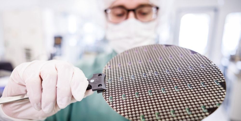
While the technological advantages of SiC are obvious due to its physical properties, the higher costs compared to established silicon continue to be an obstacle to even faster market penetration. Chip costs are more than three times higher than for silicon. The SiC output wafer is the biggest cost driver here. In the case of a SiC-based metal-oxide-semiconductor field-effect transistor (MOSFET), this accounts for more than 40 percent of the manufacturing costs. In addition, due to the unfavorable mechanical material properties and large thickness of the single-crystalline SiC wafer, the electronics processed from it only achieve around 30 percent of the thermomechanical service life compared to silicon. This disadvantage leads to a chip area that is around 25 percent larger and, in the case of an inverter for example, to around 25 percent higher costs in the application.
Cost-effective SiC substrates without sawing and grinding
In the three-year ThinSiCPower project (2024-2027), funded by the Fraunhofer internal “PREPARE” program, researchers are developing an alternative way to produce cost-effective SiC substrates and significantly thinner SiC chips using more resource-efficient processing technologies. The expensive and high-quality SiC wafers are not first sawn with the usual loss of material and then later ground thin again in component processing, but the SiC crystal is separated directly into thinner wafers using a special laser process without any major loss of material, which are then bonded onto an inexpensive carrier substrate based on polycrystalline SiC. This allows significantly more wafers to be produced from one crystal. Furthermore, the so-called poly-SiC offers significantly more advantageous mechanical material properties compared to the monocrystalline substrate isotrope, which has a positive effect on the thermomechanical load cycle stability. The significantly thinner overall structure also ensures better heat dissipation.
With ThinSiCPower to the complete SiC process line, made in Germany
The institutes Fraunhofer ISE, ENAS and IWM as well as Fraunhofer IISB as project coordinator are pooling their respective expertise in ThinSiCPower. A SiC coating technology developed by Fraunhofer IISB is being adapted for the production of the poly-SiC carrier substrates, which is more cost- and resource-efficient than the conventional production method using chemical vapor deposition. The low-loss separation of the thin SiC wafers is carried out using a laser for defined mechanical pre-damage (Fraunhofer ISE) and subsequent separation under well-defined mechanical conditions for controlled crack propagation (Fraunhofer IWM). The wafer bonding process for the poly-SiC substrate with the chopped SiC, including the necessary surface preparation before and after the bonding process, is developed at Fraunhofer ENAS, while the subsequent device processing and qualification is again carried out at Fraunhofer IISB. The partners are also developing adapted electrical test methods at thin wafer level and physics-of-failure simulation models to maximize market acceptance of this new class of low-cost SiC substrates. The aim is to achieve broad applicability in the relevant industries.
The development of technology for the production of cost-effective thin SiC wafers and poly-SiC carrier substrates is intended to reduce SiC component costs by 25 percent. In addition, SiC design costs are to be reduced by a further 25 percent by increasing the load cycle stability by 300 percent. The target markets are semiconductor and power module manufacturers as well as their process and equipment suppliers through to test equipment suppliers. The partner institutes involved in the project are also pooling their expertise to set up a complete, highly innovative and future-proof SiC processing line within the Research Fab Microelectronics Germany (FMD). The consortium receives advisory support directly from industry partners.
The ThinSiCPower project not only accelerates the market penetration of silicon carbide through the targeted cost reduction and conceptual advantages, but also serves to secure an innovative, resilient and industry-relevant SiC technology value chain in Germany and Europe.
– – – – – –
Further links
👉 www.enas.fraunhofer.de
Photo: Daniel Karmann / Fraunhofer IISB