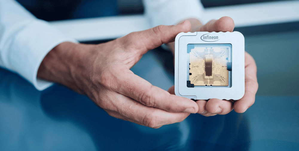
Cryogenic testing has traditionally been associated with research laboratories, where scientists and engineers characterize individual components at extremely low temperatures. However, with the advancement of quantum computers, superconducting electronics, cryogenic CMOS, and other cutting-edge semiconductor technologies, cryogenic characterization is becoming increasingly important as part of the development process.
Today, demonstrating that a device can function at cryogenic temperatures is often just the starting point. Development teams also need sufficient high-quality data to understand how devices behave across an entire wafer, identify process variations, validate designs, establish manufacturing controls, and determine whether a technology is ready for scaling.
This shift is moving cryogenic characterization from the research lab closer to the production line, making automated wafer-level testing increasingly important.
Why Cryogenic Data at the Wafer Level Is Important
A handful of successful devices can prove that a technology works. What they cannot reveal, however, is whether the underlying semiconductor process is consistent enough to support large-scale production. Answering this question requires data—and usually a great deal more of it.
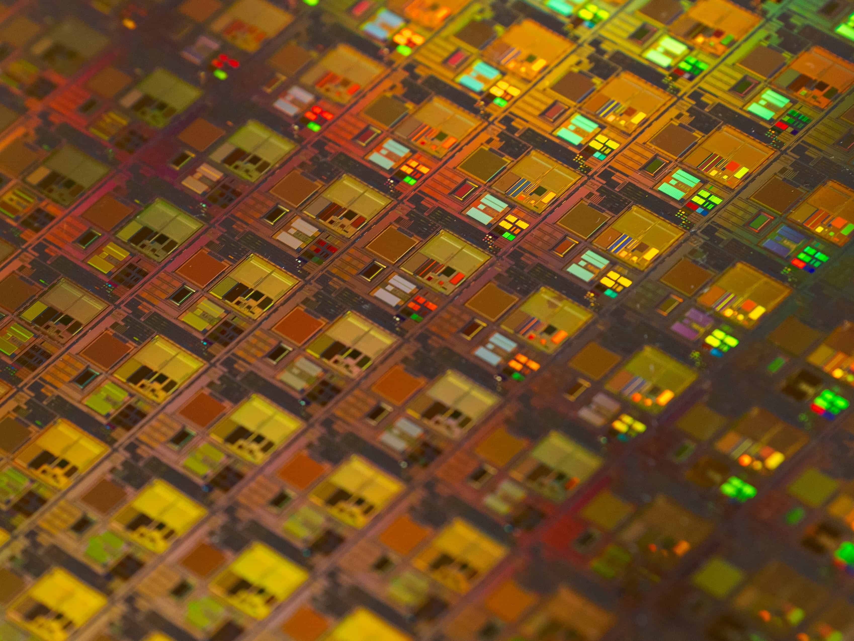
Wafer-level cryogenic characterization enables engineers to collect measurement data across much larger device populations. Instead of looking at isolated results, development teams can identify distributions, wafer-level trends, process variations, and outliers that might never come to light when testing only a few devices.
Companies can use these data sets to:
- accelerate process development and gain insights into yield
- validate process design kits (PDKs)
- define cryogenic design rules and operating margins
- implement process control monitoring
- correlate device behavior at room temperature and under cryogenic conditions
- support wafer-level screening and sorting
This becomes particularly important as the technology nears market readiness. The question is then no longer, “Can we manufacture a functioning device?” but rather: “Can we manufacture devices that consistently operate within the required specifications?”
Wafer-level characterization provides engineering teams with the statistical foundation they need to answer this question with confidence.
The requirements for cryogenic testing change as technologies mature
There is no single cryogenic test strategy that is suitable for every semiconductor development program. What a team needs in the early stages of development can differ significantly from the requirements that arise as the technology approaches mass production.
Early-stage programs may focus on device validation, material evaluation, measurement methodology, or proof-of-concept testing. At this stage, flexibility and access to expertise in cryogenic measurements can be just as important as test throughput. Engineers may still be exploring device behavior, refining measurement techniques, or determining which parameters provide the most useful insights.
As programs mature, requirements change. Instead of thoroughly characterizing a few devices, teams may need to measure hundreds or thousands of structures across multiple wafers. Repeatability, automation, throughput, and data management become significantly more important as engineers now seek to build statistically meaningful datasets.
Production-oriented cryogenic wafer testing can support process optimization, PDK validation, process control monitoring, manufacturing readiness, and wafer-level screening. These applications require a test environment capable of delivering consistent measurements at a scale for which conventional laboratory workflows are not designed.
The Challenge of Building In-House Cryogenic Test Capabilities
Building these capabilities in-house can be a major undertaking. Cryogenic testing at the wafer level involves much more than simply cooling a device and taking a measurement. Companies may require specialized cryogenic equipment, wafer-testing capabilities, measurement instruments, automation software, suitable facilities, clearly defined measurement procedures, and engineers who are knowledgeable in both semiconductor characterization and cryogenic testing.
For companies with established, long-term cryogenic testing needs, building such an infrastructure may make sense. For development teams looking to advance a program, however, the time and investment required to build internal capabilities can become a bottleneck in itself.
This is where cryogenic testing services offer an alternative. By utilizing an established environment for cryogenic characterization, teams can begin collecting the necessary data without first having to build the entire testing infrastructure themselves. In addition, they can draw on expertise in the field of cryogenic measurement technology, even if their test methodologies and requirements may still be under development.
Accelerating Development with the Advanced Cryogenics Lab
FormFactor’s Advanced Cryogenics Lab is designed to support customers at various stages of this development process through both “Applications Exploration” and “Production Test Services.”
“Applications Exploration” supports programs that are still grappling with technical issues, measurement approaches, component behavior, and characterization requirements in the early stages. Engineering teams can collaborate with experts in cryogenic measurement technology as they refine their technologies and determine the appropriate test methods.
Production test services are geared toward the next phase, when companies require larger data sets and more scalable wafer-level characterization.
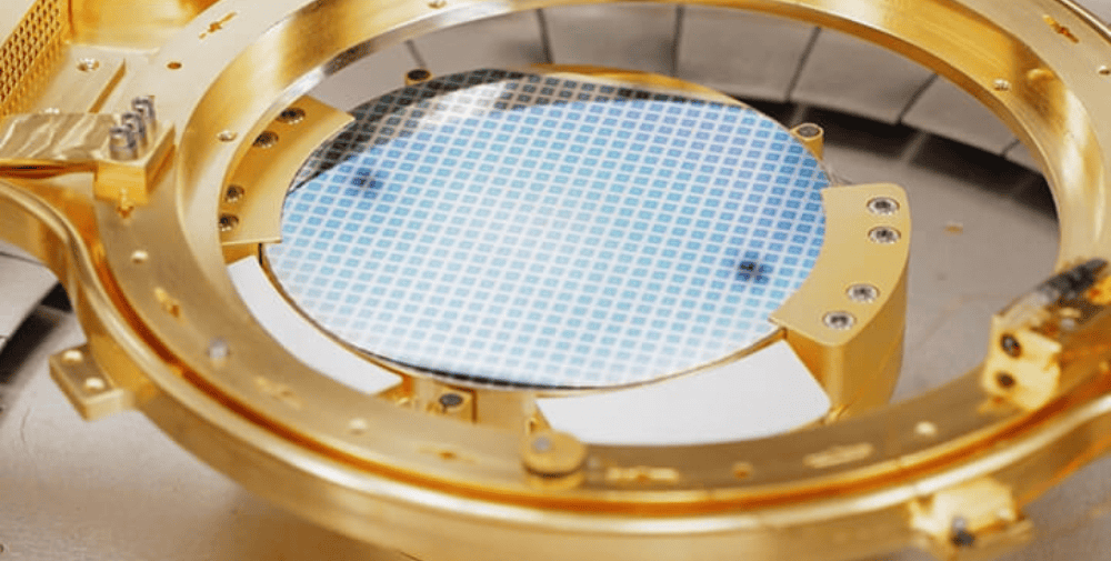
For wafer-scale applications with a focus on manufacturing, the Advanced Cryogenics Lab’s IQ3000 platform supports automated wafer-level measurements on 150-mm and 200-mm wafers over a temperature range from 4 K to 120 K.
This enables development teams to go beyond measuring individual devices and capture the larger datasets required for process development, yield data collection, statistical process characterization, manufacturing readiness, and production-scale cryogenic testing.
Automation is particularly important at this stage. When hundreds or thousands of structures need to be characterized, manually repeating the same measurement process is simply not feasible. Automated wafer-level testing makes it possible to collect more data while ensuring the measurement consistency that engineers need to compare results across different devices and wafers.
Relationship Between Performance at Room Temperature and at Low Temperatures
Another valuable application of cryogenic wafer-level characterization is understanding the relationship between measurements at room temperature and device performance at low temperatures.
If engineers can identify meaningful correlations between the two, room-temperature wafer test data may provide useful insights into subsequent behavior at low temperatures. Over time, these correlations could help teams identify useful screening criteria, understand process signatures, and determine which parameters deserve special attention during cryogenic characterization.
However, to determine these relationships, sufficient data is needed to distinguish true trends from normal variations between individual devices. This is another reason why wafer-level characterization is gaining value as semiconductor technologies mature. Engineers can evaluate behavior across statistically meaningful device populations rather than drawing conclusions from a small number of individual measurements.
Bridging the Gap Between Research and Manufacturing
The transition of a semiconductor technology from research to manufacturing changes the questions engineers must answer. In the early development phase, the focus is on whether a device works at all. In manufacturing, the focus shifts to whether a process can produce devices that operate consistently, predictably, and within defined specifications.
Cryogenic semiconductor technologies are now facing this same transition. As quantum, superconducting, cryogenic CMOS, and related technologies approach commercial deployment, development teams need larger and more reliable datasets to understand process variations, improve yield, validate designs, and establish manufacturing controls.
Cryogenic characterization at the wafer level can help bridge this gap. By combining expertise in cryogenic measurements with automated wafer-level testing and scalable data acquisition, FormFactor’s Advanced Cryogenics Lab offers development teams the ability to obtain the necessary characterization data without first having to build a complete cryogenic test environment in-house.
This can help shorten the path from demonstrating a technology in the lab to understanding the requirements for its mass production.
Frequently Asked Questions: Wafer-Level Cryogenic Characterization
What is wafer-level cryogenic characterization?
Wafer-level cryogenic characterization is the process of measuring semiconductor devices directly on a wafer at very low temperatures. Instead of testing only a few individual devices, wafer-level characterization enables engineers to collect data across larger groups of devices to better understand performance, variation, and process behavior.
Why is wafer-level cryogenic testing important?
Testing a larger number of devices provides engineers with the statistical data needed to identify process variations, detect outliers, establish operating margins, validate designs, and assess production readiness. This is becoming increasingly important as cryogenic semiconductor technologies make the transition from research to commercialization.
What types of technologies require cryogenic semiconductor testing?
Cryogenic characterization can support the development of technologies, including quantum computing devices, superconducting electronics, cryogenic CMOS, and other semiconductor devices designed for operation at low temperatures.
How do cryogenic wafer tests contribute to yield improvement?
Wafer-level testing helps engineers understand how device performance varies across larger populations and across the entire wafer. These data sets can be used to identify outliers, understand process variations, gain insights into yield, and determine where process improvements may be needed.
Can the results of wafer testing at room temperature be correlated with performance at cryogenic temperatures?
Yes, one goal of large-scale characterization may be to investigate correlations between measurements at room temperature and device behavior at cryogenic temperatures. To identify meaningful correlations, sufficient measurement data is required to distinguish significant trends from normal variations between individual devices.
What wafer sizes and temperatures does the IQ3000 support?
FormFactor’s IQ3000 platform supports automated wafer-level measurements for 150-mm and 200-mm wafers at temperatures ranging from 4 K to 120 K. This enables large-scale characterization for process development, statistical analysis, manufacturing readiness, and production-oriented testing.
Why should you use cryogenic testing services instead of setting up your own lab?
Establishing an in-house cryogenic wafer testing capability may require specialized equipment, facilities, automation, measurement protocols, and technical expertise. Cryogenic testing services provide development teams with access to established characterization capabilities and expertise without having to build the entire testing environment from scratch.
– – – – –
Related Links
👉 www.formfactor.com
Photo: FormFactor