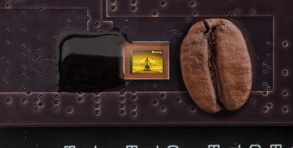
There is rapid development in the market for the microdisplays used in augmented reality (AR), virtual reality (VR) and mixed reality (MR) applications (often collectively referred to as XR) and this will be an important growth market of the future. The integration of OLED and µLED frontplane technologies in CMOS backplanes is not only the key to success in this sector but also the technological basis for near-to-eye visualization of information. Fraunhofer IPMS and Fraunhofer FEP have now decided, in consultation with the Fraunhofer-Gesellschaft, to integrate the Fraunhofer FEP Microdisplays and Sensors business unit into Fraunhofer IPMS. Their goal is to leverage synergies in the area of infrastructure, pool expertise and establish a unique profile for both institutes. Fraunhofer IPMS has long been one of the leading institutes in microelectronics and microsystems engineering.
Over the past ten years, the Microdisplays and Sensors business unit has developed into a globally successful and established player under the umbrella of Fraunhofer FEP. At the current stage of development, the transfer to an institute specialized in microelectronics offers suitable conditions to further develop the business unit. This will also allow Fraunhofer FEP, as a process-oriented institute, to focus even more on its expertise in electron beam and plasma technology. This transfer provides technological solutions for the growing demand in the fields of energy, sustainability, life sciences and environmental technologies for industry and society – now and in the future.
“By integrating the Fraunhofer FEP Microdisplays and Sensors business unit into Fraunhofer IPMS, we are pooling our expertise and ensuring the best possible use of our infrastructure. This will also increase our chances to win projects with the Microelectronics group. The transfer is a good example of the strategic development of a research field and the leveraging of synergies across institutes,” says Prof. Holger Hanselka, President of the Fraunhofer-Gesellschaft.