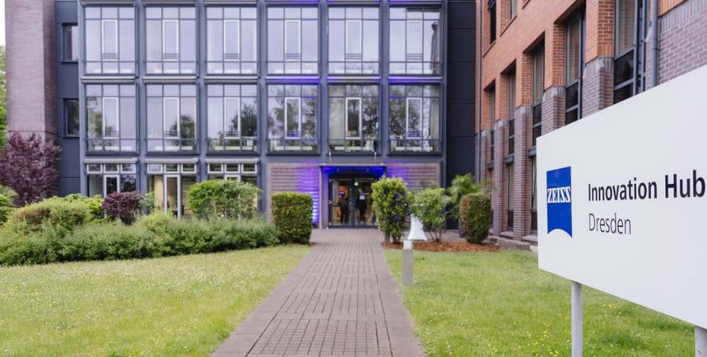
The new facility is located in Dresden, the center of semiconductor innovation in Europe. This enables close collaboration with customers and partners from the semiconductor industry in physical defect analysis, the development of new materials and the improvement of process yields for current logic and memory technologies, power semiconductors, MEMS, advanced packaging and other fields of application. In Dresden, ZEISS Microscopy will address the increasing automation of microscopy workflows and new methods to help the semiconductor industry accelerate root cause analysis and solution finding for the most challenging problems in microelectronics.
The Dresden lab is ZEISS’ third major investment in semiconductor microscopy applications and strengthens the company’s global support capabilities. The team in Dresden works closely with its counterparts in Taiwan and Korea to share knowledge and best practices to best meet the needs of customers in the three global hotspots of semiconductor excellence. The advanced applications developed by these three teams will shape ZEISS’ innovation roadmap to tackle the biggest challenges facing laboratory experts in the semiconductor industry.
The ZEISS Microscopy Semiconductor Applications Lab is located in the ZEISS Innovation Hub Dresden, which opened in May. The location complements the ZEISS Innovation Center in Hsinchu Science Park, Taiwan, which opened in June 2024 and has an extensive portfolio for the productivity needs of semiconductor research, development, production and failure analysis. The third innovation center is located in Dongtan, Korea, where the company is developing applications with an extensive inventory of optical and electronic equipment, X-ray microscopes and high-resolution CT and 3D measurement instruments.
About ZEISS
ZEISS is a global technology leader in the optical and optoelectronic industry. In its four divisions Semiconductor Manufacturing Technology, Industrial Quality & Research, Medical Technology and Consumer Markets, the ZEISS Group most recently generated annual sales of 10 billion euros (September 30, 2023).
ZEISS develops, produces and distributes highly innovative solutions for industrial metrology and quality assurance, microscopy solutions for life sciences and materials research as well as medical technology solutions for diagnostics and therapy in ophthalmology and microsurgery for its customers. ZEISS also stands for the world’s leading lithography optics, which are used by the chip industry to manufacture semiconductor components. ZEISS branded products such as ophthalmic lenses, photographic lenses and binoculars are sought-after and trendsetters worldwide.
With a portfolio geared towards future growth areas such as digitalization, health and Industry 4.0 and a strong brand, ZEISS is helping to shape technological progress and is advancing the world of optics and related areas with its solutions. The basis for the success and further continuous expansion of ZEISS’ technology and market leadership is the sustained high level of expenditure on research and development. ZEISS invests 15% of its revenue in research and development work – this high level of expenditure has a long tradition at ZEISS and is also an investment in the future.
With more than 44,000 employees, ZEISS is active in around 50 countries with more than 60 sales and service locations, 35 research and development locations and 35 production locations worldwide (as of March 31, 2024). The headquarters of the company, which was founded in Jena in 1846, is located in Oberkochen, Germany. The sole owner of the parent company, Carl Zeiss AG, is the Carl Zeiss Foundation, one of the largest German foundations for the promotion of science.
ZEISS Research Microscopy Solutions
ZEISS Research Microscopy Solutions is the leading provider of light, electron and X-ray microscope systems, correlative microscopy and software solutions that utilize AI technologies. The portfolio includes products and services for life sciences, materials and industrial research as well as for education and clinical practice. The division is headquartered in Jena. Further production and development sites are located in Germany, the UK, the USA and China. ZEISS Research Microscopy Solutions is part of the Industrial Quality & Research division.
– – – – – –
Further links
👉 www.zeiss.de
👉 www.zeiss.de/mikroskopie
Photo: ZEISS


