2D quantum material instead of silicon
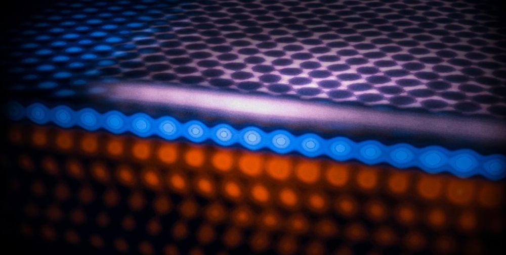
Schematic representation showing the protective function of a graphene layer against water. The electrical current flow at the edge of the topological insulator indene remains completely unaffected by environmental influences.
Modern computer chips are becoming ever faster and more powerful. This works because their basic building blocks, the transistors, are becoming ever smaller and more compact. In a few years, they will only be a few atoms in size. By then, however, the miniaturization of the silicon technology used to date will have reached its physical limits. This is why the search for alternative materials with completely new properties is the basis for future technological growth.
Scientists from the Cluster of Excellence ct.qmat – Complexity and Topology in Quantum Matter at the Universities of Würzburg and Dresden discovered topological quantum materials such as indenes as early as 2021, which have enormous potential for ultra-fast and low-consumption electronics. The extremely thin quantum semiconductors consist of just a single layer of atoms – in the case of indene, these are indium atoms – and, as topological insulators, conduct electricity at their edges with virtually no braking.
“Such a single atomic layer must be produced in complex vacuum apparatuses and on a specific carrier material. In order to produce electronic components from it, the two-dimensional material would have to be removed from the vacuum. However, even the slightest contact with air, for example, causes the layer to oxidize. This destroys its revolutionary property and makes it unusable,” explains experimental physicist Prof. Ralph Claessen, Würzburg spokesperson of the Cluster of Excellence ct.qmat.
The Würzburg ct.qmat team has now been able to solve this problem. The results were published in the journal Nature Communications.
Protective layer sought …
“We spent two years researching a way to shield the sensitive indene layer from environmental influences with a protective layer. The difficulty was that the protective layer itself was not allowed to react with the indene layer,” says Cedric Schmitt, a Claessen doctoral student involved in the project. This is because when two different atoms, such as those of the protective layer and the semiconductor to be protected, come into contact, a chemical reaction takes place at an atomic level that changes the material. This is not a problem with conventional silicon chips because silicon consists of many atomic layers and there are always enough untouched, functional ones left.
“A semiconductor material consisting of a single atomic layer such as indene would be destroyed by a protective film at the same time. A seemingly unsolvable problem that has awakened our spirit of research,” says Claessen. The search for a usable protective layer began with van der Waals materials, named after the Dutch physicist Johannes Diderik van der Waals (1837 – 1923). “The two-dimensional van der Waals atomic layers have the great property that their atoms are strongly bonded to each other, but only lie weakly on the carrier material,” explains Claessen. “A similar principle is used when writing with a pencil whose lead is made of graphite – a modification of carbon whose atoms form honeycomb-shaped layers. The individual graphene layers can be removed very easily. We needed something like that!”
… and found it!
In an elaborate ultra-high vacuum apparatus, the Würzburg research team finally heated silicon carbide (SiC) as a carrier material for indene – and investigated the conditions under which graphene is formed from it. “Silicon carbide is made up of silicon and carbon. When heated, the carbon atoms detach from the surface and form graphene,” says doctoral student Schmitt, explaining what happens in the laboratory. “We then vapor-deposited indium atoms, which are immersed between the protective graphene layer and the supporting carbide layer. This is how the protective layer for our two-dimensional quantum material indene was created.”
Awning stretched
The Würzburg ct.qmat team led by Claessen has thus succeeded for the first time in the world in experimentally producing a functional protective layer for a two-dimensional quantum semiconductor material without destroying its extraordinary quantum properties. After analyzing the manufacturing process, the scientists examined in detail whether the layer actually protects against oxidation and corrosion. “It works! We can even expose the sample to water and nothing happens to it,” says Claessen happily. “The graphene layer is like an umbrella for our indene.”
On the way to atomic layer electronics
The research results open up exciting application prospects for the extremely sensitive semiconductor atomic layers. The production of ultra-thin electronic components requires them to be processed in air or in other chemical environments. With the protection that has now been discovered, a principle has been found that makes this possible. The Würzburg scientists are now concentrating on discovering further van der Waals materials that also fulfill this protective function. They already have a few candidates in mind. Because even though graphene efficiently protects atomic monolayers from environmental influences, it is itself electrically conductive and can therefore cause short circuits.
The Würzburg scientists are working on overcoming these challenges and creating the conditions for future atomic layer electronics.
Publication
Achieving environmental stability in an atomically thin quantum spin Hall insulator via graphene intercalation device
Cedric Schmitt, Jonas Erhardt, Philipp Eck, Matthias Schmitt, Kyungchan Lee, Philipp Keßler, Tim Wagner, Merit Spring, Bing Liu, Stefan Enzner, Martin Kamp, Vedran Jovic, Chris Jozwiak, Aaron Bostwick, Eli Rotenberg, Timur Kim, Cephise Cacho, Tien-Lin Lee, Giorgio Sangiovanni, Simon Moser, Ralph Claessen
Nat Commun 15, 1486 (2024). https://doi.org/10.1038/s41467-024-45816-9.
Cluster of Excellence ct.qmat
The Cluster of Excellence ct.qmat – Complexity and Topology in Quantum Matter has been jointly funded by Julius-Maximilians-Universität (JMU) Würzburg and Technische Universität (TU) Dresden since 2019. More than 300 scientists from more than 30 countries and four continents are researching topological quantum materials that reveal surprising phenomena under extreme conditions such as ultra-low temperatures, high pressure or strong magnetic fields. The Cluster of Excellence is funded as part of the Excellence Strategy of the German federal and state governments – the only cluster in Germany that spans several federal states.
As a University of Excellence, the Technische Universität Dresden (TUD) is one of the most powerful research institutions in Germany. With around 8,300 employees and around 29,000 students in 17 faculties, it is one of the largest technically-oriented universities. Founded in 1828, today it is a globally oriented, regionally anchored top university that aims to make innovative contributions to solving global challenges. In research and teaching, it combines engineering and natural sciences with the humanities, social sciences and medicine. This nationally outstanding diversity of subjects enables the university to promote interdisciplinarity and bring science into society.
Contact
Prof. Ralph Claessen
Würzburg spokesperson of the Cluster of Excellence ct.qmat
Julius-Maximilians-Universität Würzburg
Tel: +49 931 318 5732
ralph.claessen@uni-wuerzburg.de
– – – – –
Further links
👉 www.tu-dresden.de
Photo: Jonas Erhardt/Christoph Maeder