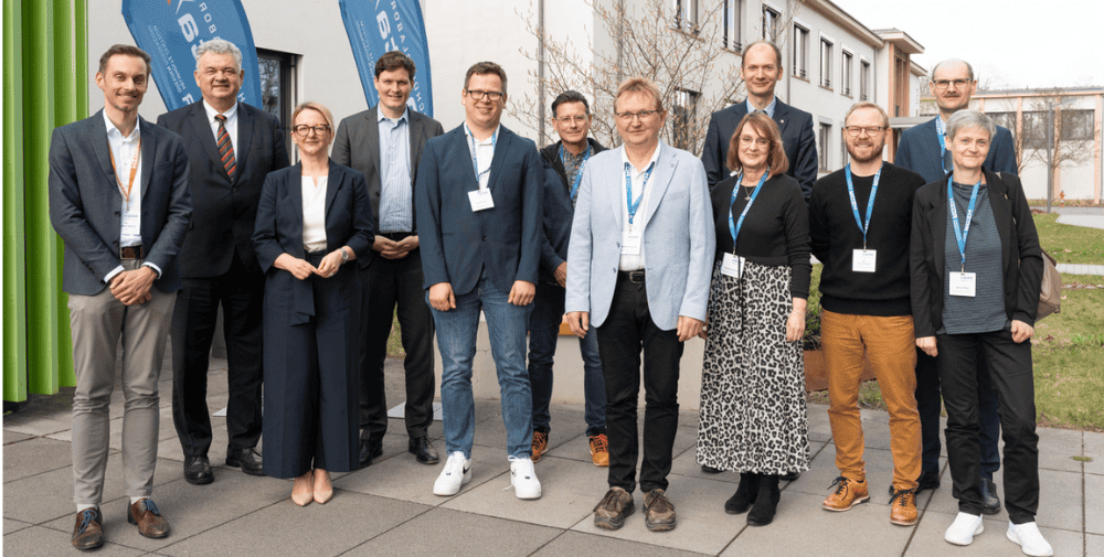
“The investment is a clear commitment to our Saxon location. In addition, the modernization helps to ensure that we continue to be one of the world’s technology leaders and, above all, it strengthens our position as the only major Western wafer manufacturer,” said Dr. Michael Heckmeier, CEO of Siltronic AG, at the opening. The Freiberg site in Saxony is one of four production locations of the group, which manufactures in Germany, Singapore and the USA.
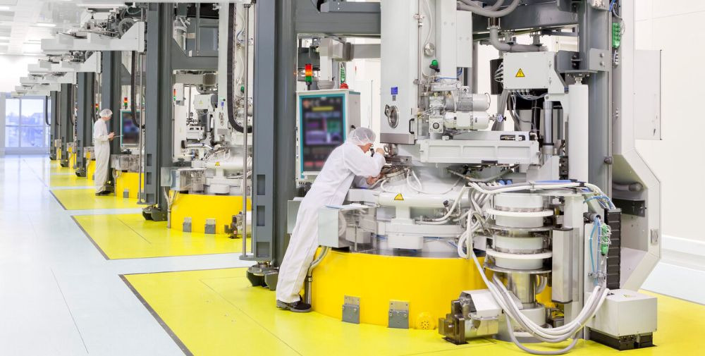
With a floor space of 20,000 square meters, the extension building is almost as large as three soccer fields. Here, man-sized silicon monocrystals are manufactured in a process that takes five to seven days. The so-called ingots have a diameter of around 300 millimeters and weigh several hundred kilograms. In a complex process under cleanroom conditions, they are processed into wafers – wafer-thin slices of silicon. Siltronic’s customers use the wafers to manufacture microchips that can be found in everyday items such as tablets, smartphones and e-cars, as well as wind turbines and aircraft. The semiconductor industry is receiving tailwind from the megatrends of artificial intelligence, digitalization and electromobility.
Siltronic has invested more than one billion euros at the site since taking over Freiberger Elektronikwerkstoffe GmbH in 1995. “With our investments, we believe we are well equipped for the future to be at the forefront of a challenging market environment,” Heckmeier explains. The site in Freiberg, Saxony, currently employs around 1,000 people.
– – – –
Further links
👉 www.siltronic.com
Photo: Siltronic
