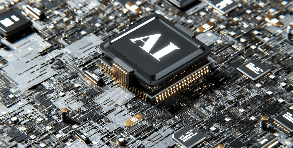
The four-year EU project, launched in March 2025, is building the European Network of Chips Competence Centres (ENCCC) and maximizing synergies between CCCs, Chips Pilot Lines (PLs) and the virtual Design Platform (DP). Under the leadership of experienced cluster organizations and technology partners, a central platform is being created that accelerates innovation, facilitates access to technology and funding for companies and strengthens Europe’s semiconductor competence on a global scale.
The CCCs, CPLs and the DP are key initiatives of the EU Chips Act, driven by the Chips JU. These initiatives provide companies – especially SMEs and start-ups – with essential resources, training and access to state-of-the-art semiconductor infrastructure. While CCCs foster innovation and specialized expertise, CPLs bridge the gap between research and production, and the DP provides a cloud-based environment with advanced design tools to support chip development in Europe.
aCCCess as the connecting link between CCCs, PLs and DP
aCCCess aims to build and strengthen the European Network of Chips Competence Centres (ENCCC). To this end, the ENCCC is organized into five focus groups: Operations and Best Practices, Public Relations and Events, Technology Offerings and Technology Transfer, Training and Skills Development, and Funding. These groups develop harmonized processes in these key areas, ensuring seamless collaboration across Europe.
aCCCess supports the development of CCCs, PLs and DP through online and face-to-face events, including an annual community event to promote cross-border collaboration.
To facilitate access to the CCCs’ services, training and technology offerings, aCCCess will create a shared online marketplace that showcases the CCCs’ service catalogs and provides AI-enabled servicing and matchmaking opportunities. In addition, investment opportunities will be promoted through a venture capital network and the Chips Finance Lab. An annual pitching event for startups will specifically focus on these funding opportunities.
In addition, aCCCess will establish its own think tank and host monthly webinars with industry experts to discuss trends, promote public-private partnerships and advance best practices in cluster management and operations. Finally, the Pilot Lines and Design Platform will offer specialized training and webinars to assist CCCs in providing resources and increasing their visibility.
The benefits of the project at a glance
Strengthen skills
- Access to CCCs, PLs and DP
- Faster processes through the aCCCess marketplace
- Early access to new technologies and best practices
Exchange with experts:inside
- Establishment and support of the “Chips Think Tank”, which emphasizes the expertise within the ENCCC
- Events for direct exchange with expert:Inside from CCCs, PLs and DP
- Direct networking with relevant actors for knowledge transfer and cooperation
Provide financing opportunities
- Connection to the Chips Finance Lab: training on financing products from EIB, EIF, etc.
- Matchmaking with investors
- Direct access to investors for business growth and project funding
- Improved chances of success in financing innovation projects
About CCCs, PLs and DP
Chips Competence Centres (CCC): Innovation centers for Europe’s semiconductor industry
The Chips Competence Centres provide companies – especially SMEs and start-ups – with resources to develop semiconductor solutions. This includes support, training and access to major infrastructure facilities established under the EU Chips Act, such as the Chips Pilot Lines and the Design Platform. Each center will reflect regional and national strengths and specialize in one or more key technology areas.
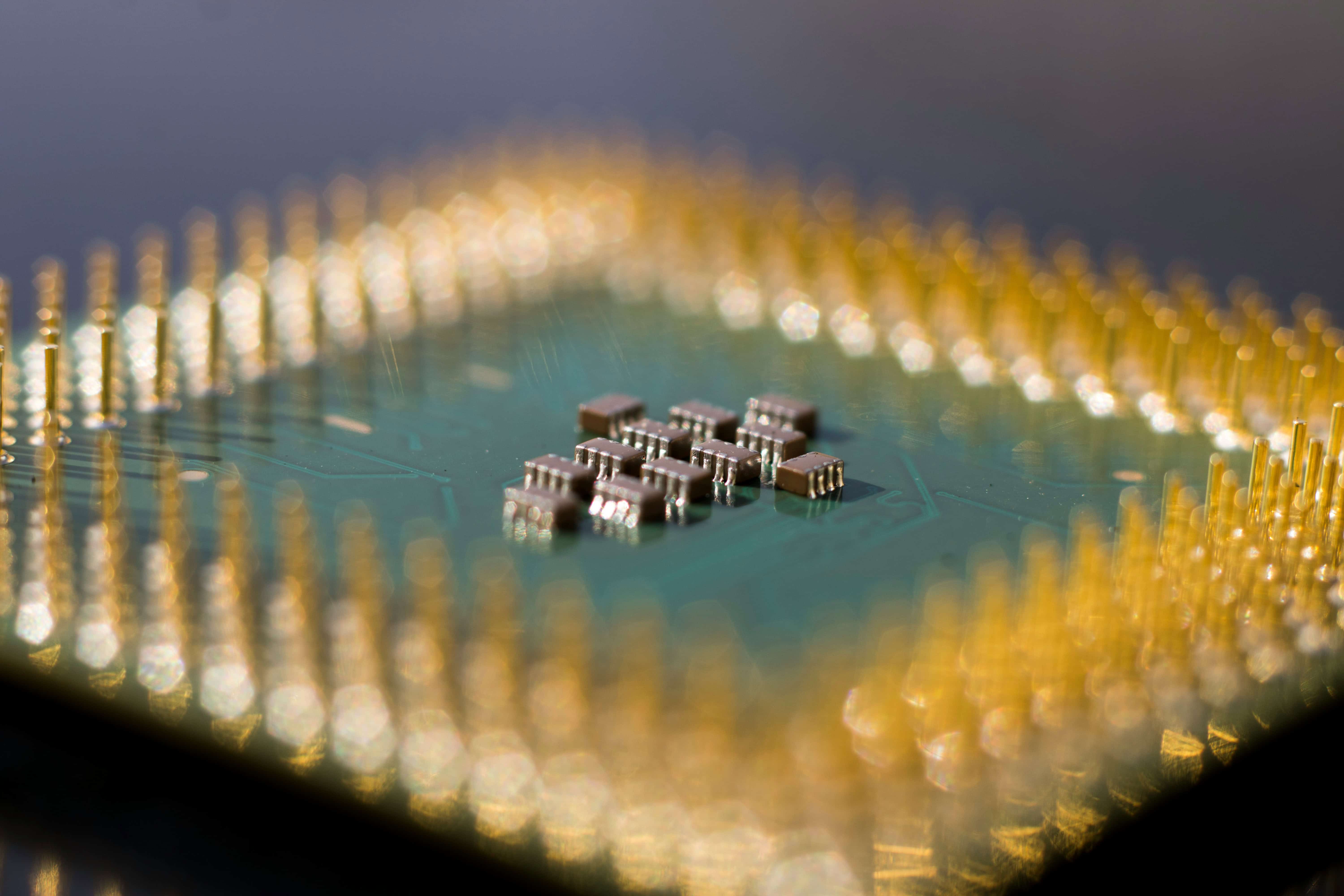
Chips Pilot Lines (PLs): From research to production
Pilot lines are designed to support companies in the areas of process development, testing, experimentation and small-scale production. This approach is intended to sustainably close the gap between laboratory research and industrial production. The pilot lines will focus on key technologies such as sub-2 nm GAA process technology, FD-SOI technology at 10 nm and below, and heterogeneous integration.
Design Platform (DP): The cloud-based future of chip design
The Design Platform will be a cloud-based virtual environment accessible across the European Union. It will offer a wide range of design tools and resources, from IP libraries to Electronic Design Automation (EDA) tools, as well as support services. The platform will be open, non-discriminatory and transparent to ensure widespread use.
Project partners
- Blumorpho
- VDI/VDE Innovation + Technik GmbH
- Minalogic
- Silicon Saxony
- Silicon Alps
- Mesap
- Czech National Semiconductor Cluster
Associated partners
- IMEC (Interuniversitair Micro-Electronica Centrum)
- Fraunhofer (Fraunhofer-Gesellschaft zur Förderung der angewandten Forschung e.V.)
- CEA (Commissariat A L’Energie Atomique Et Aux Energies Alternatives)
- FTMC (Valstybinis Moksliniu Tyrimu Institutas Fiziniu Ir Technologijos Mokslu CentraS) (Center for Physicals Sciences and Technology)
- PPTF (Polska Platforma Technologiczna Fotonik)
- UL (UNIVERZA V LJUBLJANI)
- AMETIC (Asociacion Multisectorial De Empresas De La Electronica, Las Tecnologias De La Informacion y La Comunicacion, De Las Telecomunicaciones Y De Los Contenidos Digitales)
- INNOVA-IRV (Fundación Instituto Ricardo Valle de Innovación)
- EIS (Ettevotluse Ja Innovatsiooni Sihtasutus) (Estonian Business and Innovation Agency – Enterprise Estonia)
- HTNL (Vereniging High Tech NL)
- TAMLINK (Tuotekehitys Oy Tamlink)
- GAIA (Association of Applied Knowledge and Technology Industries in the Basque Country)
- AENEAS (Association for European NanoElectronics ActivitieS)
- EPoSS (European Association on Smart Systems Integration)
- INSIDE (Industry Association)
– – – – –
Further links
https://silicon-saxony.de/leistungen/projekte/acccess/