Polished silicon wafers are a common solution for the growth of GaN due to their cost efficiency and good availability compared to alternatives such as silicon carbide (SiC) and sapphire. However, SOI wafers are gaining traction due to their superior device isolation, reduced parasitic capacitance and improved thermal stability – key advantages for power devices. While GaN-on-Si and GaN-on-SiC growth technologies remain the established choice for high power applications, bonded SOI structures are emerging as a promising alternative. These structures offer a unique advantage in device integration as GaN growth technologies evolve and enable more efficient and scalable device fabrication. Recent collaboration with the Interuniversity Microelectronics Centre (IMEC) has yielded promising results, highlighting in particular the potential of SOI wafers for GaN growth.
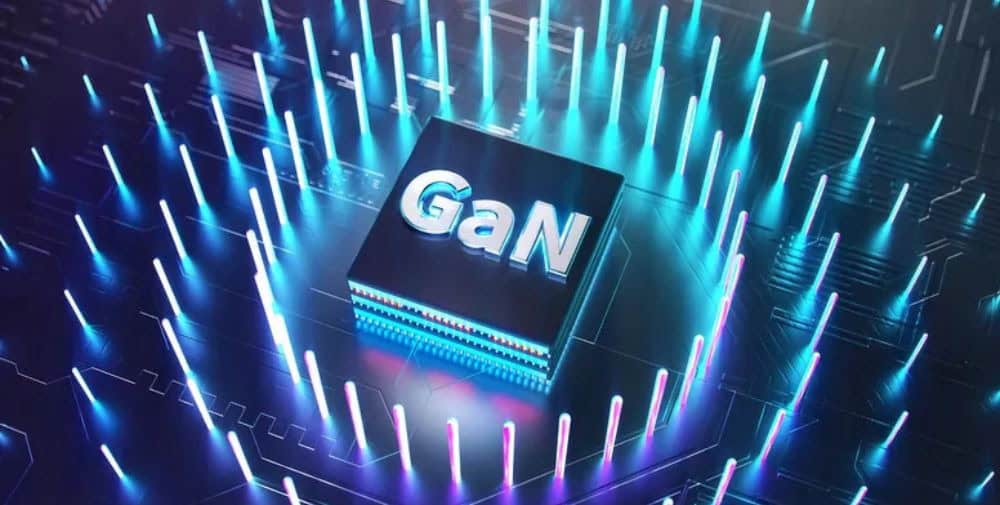
Silicon substrate wafers for gallium nitride growth
Okmetic Power’s GaN substrate wafers, polished on one and both sides, are specifically designed to meet the demanding requirements of GaN epitaxy. These wafers are designed to reduce wafer curvature and deformation while improving durability. The robustness of our Power GaN substrates is supported by our Advanced Magnetic Czochralski (A-MCz®) crystal growth process, which enables ultra-high concentration doping and optimized interstitial oxygen (Oi) sites. This process not only strengthens the lattice structure but also enables precise orientation control, ensuring excellent stress management.
Designed for flexibility, Okmetic Power GaN substrates can be fully customized to meet the specific requirements of a variety of GaN applications. These substrates are available in <111> orientation and support high voltage GaN HEMT devices (over 650 V) and high power LEDs. For applications requiring improved durability, thicknesses up to 1,150 µm are available to further reduce deflection and deformation. Optional poly and LTO backsides provide additional resilience.
IMEC validates GaN SOI substrate wafers for high-quality GaN epitaxy
In a recent study by IMEC, Okmetic’s GaN-optimized and non-optimized SOI wafers were evaluated and their effects on GaN growth, wafer deflection and stability were compared. IMEC successfully grew a 4.4 µm GaN epi-stack on Okmetic wafers, with the GaN-optimized SOI wafers demonstrating superior GaN layer uniformity, reduced wafer bow and improved electrical performance in post-growth studies. Electrical performance tests by IMEC, including buffer breakdown, Hall measurements and dispersion analysis, show that Okmetic Power GaN SOI substrate wafers offer comparable performance to industry-leading materials used as reference in the study.
The study confirms the stability and suitability of Power GaN SOI substrate wafers for high power applications. They offer both high electrical reliability and exceptional performance under high-temperature conditions, which are critical for long-term durability and efficiency in demanding applications.
Specifications of the SOI substrate wafers
Both GaN-optimized and non-optimized SOI wafers had identical specifications for the device and buried oxide layers, as well as for the thickness of the handle layer. Both also used a <111>crystal orientation, which is known to improve wafer durability. The main difference between the two wafer types lies in the GaN-optimized SOI wafers, which have a higher doping and interstitial oxygen (Oi) concentration in the handle layer. This optimization significantly improves the robustness and stability of the wafer during the high-temperature GaN growth process and provides an ideal platform for GaN epitaxy without compromising structural integrity.
In addition, Okmetic GaN SOI substrate wafers provide excellent isolation properties for monolithic GaN integration, reducing parasitic capacitance and leakage currents – critical factors for high frequency and power applications.
Improved wafer stability, electrical performance and device reliability
The SOI wafers optimized for Power GaN exhibit exceptional stability, showing minimal bowing, no edge defects and consistent GaN layer quality, ensuring reliability in high-temperature processes. This stability is crucial for GaN growth, as mechanical and thermal stresses are a challenge.
Electrical tests confirm the suitability of the wafers for high-performance GaN devices with high buffer breakdown voltages (750 V in reverse bias, 850 V in forward bias) and minimal effects of trapped charge, as demonstrated by dispersion measurements. In addition, the uniform AlGaN cap layer with minimal thickness deviations ensures stable 2DEG properties and reliable threshold voltage in GaN HEMTs, supporting long-term reliability and performance in advanced power applications.
– – – – – –
Further links
👉 www.okmetic.com
Photo: Okmetic