Thomas Schmidt
Managing Director AMTC
What are photomasks?
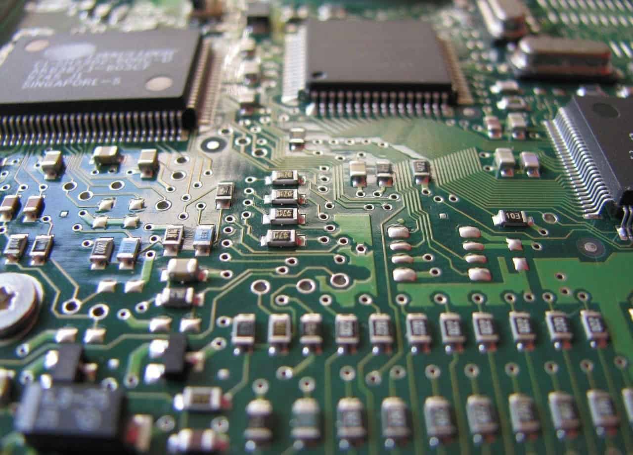
Photomasks (English “reticle”) are projection templates whose main application is photolithographic patterning in the manufacture of microelectronic circuits or microsystems. In this process, a photomask is placed over a light-sensitive material to project a specific pattern onto it. In the semiconductor industry, this is done using complex lithography exposure machines (called scanners). In this process, the structures are transferred from the photomask to a photoresist on the wafer at a 4-fold reduction in size. The pattern, the so-called “design” or “layout”, is provided by the customer. Photomasks usually consist of high purity quartz glass with different coatings, so-called blanks, depending on the application. The masks are produced using an electron beam writer. This writes the desired layouts onto a coating system on the blank. In a subsequent developer step, the exposed areas are made detachable and removed. A subsequent etching step structures the coating, with the varnish again having a masking effect. Depending on the mask type, several lithography and etching steps are necessary. Since the quality requirements for a mask are very high, a large part of the production time is spent on characterization. Mask parameters such as structure sizes, structure placement accuracy, and finding flaws (defects) that can then in turn be repaired are essential. To achieve this, there are great demands on the stability and cleanliness of the processes as well as the production environment. Besides the classical photomasks for the chip industry from 130nm to 12nm, as well as EUV, the AMTC also produces special masks. These special masks are used by research and technology organizations, equipment manufacturers (OEM), or in areas of optical elements, calibration marks, and in nano-imprint technology.
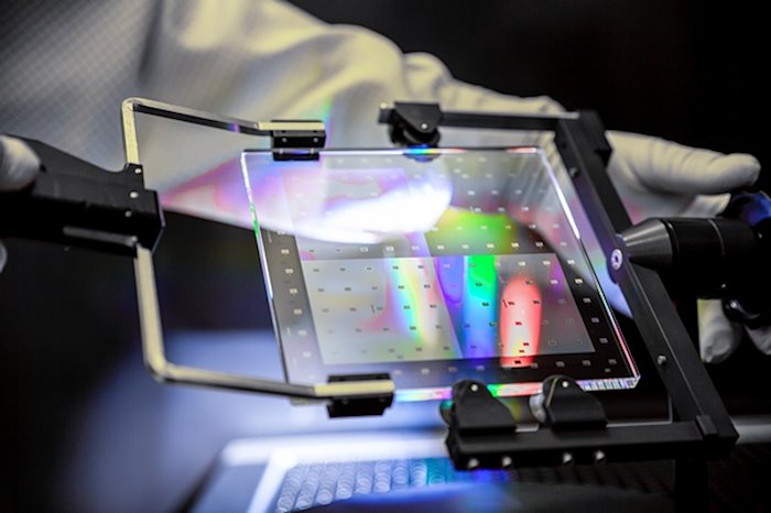
An AMTC photomask in production. Photo: AMTC
What is their importance for semiconductor manufacturing?
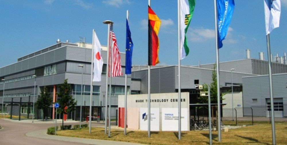
They are indispensable. That is why the Advanced Mask Technology Center GmbH & Co. KG (AMTC) was founded, which is a joint venture of GlobalFoundries (GF) and Toppan Photomasks (TP), Inc. With the AMTC, Europe’s leading center for the development and production of photolithography masks was established in Dresden in 2002. Such a technology alliance of leading companies in the semiconductor industry for the joint development and production of masks, as in the AMTC, is unique worldwide. In particular, we manufacture the masks for our partner GF’s 300mm manufacturing facilities located around the world. With the high quality masks of the AMTC we enable in particular the production of 12/14nm and 22nm FDX technology. For Toppan’s European and global customers, the AMTC provides masks for many application areas of different technology nodes. This includes technologies from 180nm down to below 10nm, including EUV. Hereby, AMTC through Toppan contributes to a robust supply chain as well as safety-related aspects for critical chip designs with its manufacturing in Europe.
In the area of dedicated masks, we provide European and international OEM customers with masks of highest requirements in a timely manner to support their development and qualification of latest devices. This strengthens the European semiconductor supply company ecosystem. We see ourselves as a critical system-relevant supplier to the semiconductor industry and in the end you can say, without masks no chips.
Photomasks are produced “just-in-time”. How do you deal with the growing demand in the future – are you already planning expansions of your manufacturing capacities?
Delays in mask manufacturing can lead to a direct production stop in the wafer fab. This is associated with high costs as well as delays. For time-critical masks, we have specified lead times of a few days. This requires good manufacturing logistics and robust processes. We know our bottlenecks in production very well and have gradually reduced them over the last few years. Here we can mention, for example, the investment in the latest electron beam recorder generations.
We serve short-term peaks in demand with the help of our partner Toppan. As a globally active mask manufacturer, Toppan operates mask houses in the USA and Asia. Via a so-called “offload”, mask orders can be transferred to other Toppan mask houses in case of capacity bottlenecks. This can run from the AMTC to the Toppan world or the other way around.
Long-term forecasts regarding mask demand are difficult. Here, we and our partners are monitoring the market to be able to react accordingly. Having massively expanded the existing cleanroom in 2019/20 to prepare for growth, there is currently still some space available to expand capacity.
Is Europe dependent on non-European players in the mask sector?
In mask production, our Dresden mask campus is the leading manufacturer in Europe and among the leading sites worldwide. However, the semiconductor industry is a global industry. Various competencies are spread across the globe and supply chains are complex. In the mask area, for example, several key players are located in Japan, producing pellicles, blanks or photoresists, among others.
In particular, in the area of mask production equipment, there are very few manufacturers. Combined with a small mask market, high investment costs are reflected in the final equipment price. Few equipment manufacturers share this limited market. These are also the large global semiconductor equipment manufacturers. Basically, as for the whole semiconductor industry, it can be said that the supply chain for mask equipment and materials within Europe is not completely autonomous. The key factor here is to manage these global supply chains very effectively. And here again, AMTC benefits from the strong global reach of its two parent companies, GlobalFoundries and Toppan.
How easy or difficult is it to build capacity? What are any bottlenecks?
As mentioned earlier, more cleanroom space is available at AMTC to increase capacity by about 25%. To be considered are long delivery times of critical production equipment of more than 12-18 months. In addition, new equipment generates a high effort for qualification. However, I think we have gained enough experience here over the last few years to integrate new equipment quickly into production. It is important to indicate higher mask requirements at an early stage. In addition to the delivery times of equipment, we see the availability of well-trained specialists and engineers as a key factor.
How important is physical proximity to customers, suppliers or even R&D?
A major advantage of physical proximity is to ensure challenging delivery times of masks to the customer. Likewise, it is an advantage to be in the same time zone to be able to coordinate technical or time-critical things. This is especially true in the R&D area. Being close to customers allows us to respond to their needs and have direct bilateral discussions. To this end, we are also involved in European funding projects in order to work out solutions together with customers.
Proximity to suppliers, especially equipment manufacturers, is equally important. To keep manufacturing running, you need short access times to service and support to get defective production equipment up and running again quickly. This is the only way to ensure short delivery times.
Photo: AMTC
__________________________________________________________________________________________________________________________________
This article was first published as part of our NEXT magazine “In Focus: Microelectronics”.
👉 Go to the complete issue of the magazine