Company type
Home | Mitglieder |
Vistec Electron Beam GmbH
Target markets
Electron-beam lithography·Lithography
Industries
Applications·Micro- / Nanoelektronics
Portfolio
Applications·Electron-beam lithography·Equipment·Lithography·Micro- / Nanoelektronics·Semiconductor Industry
Certificates
Contact
Ilmstraße 4
07743 Jena
07743 Jena
+49 3641 7998 0
Contact Person
Ines Stolberg
+49 3641 7998 155
Manager Marketing & Sales
About this member
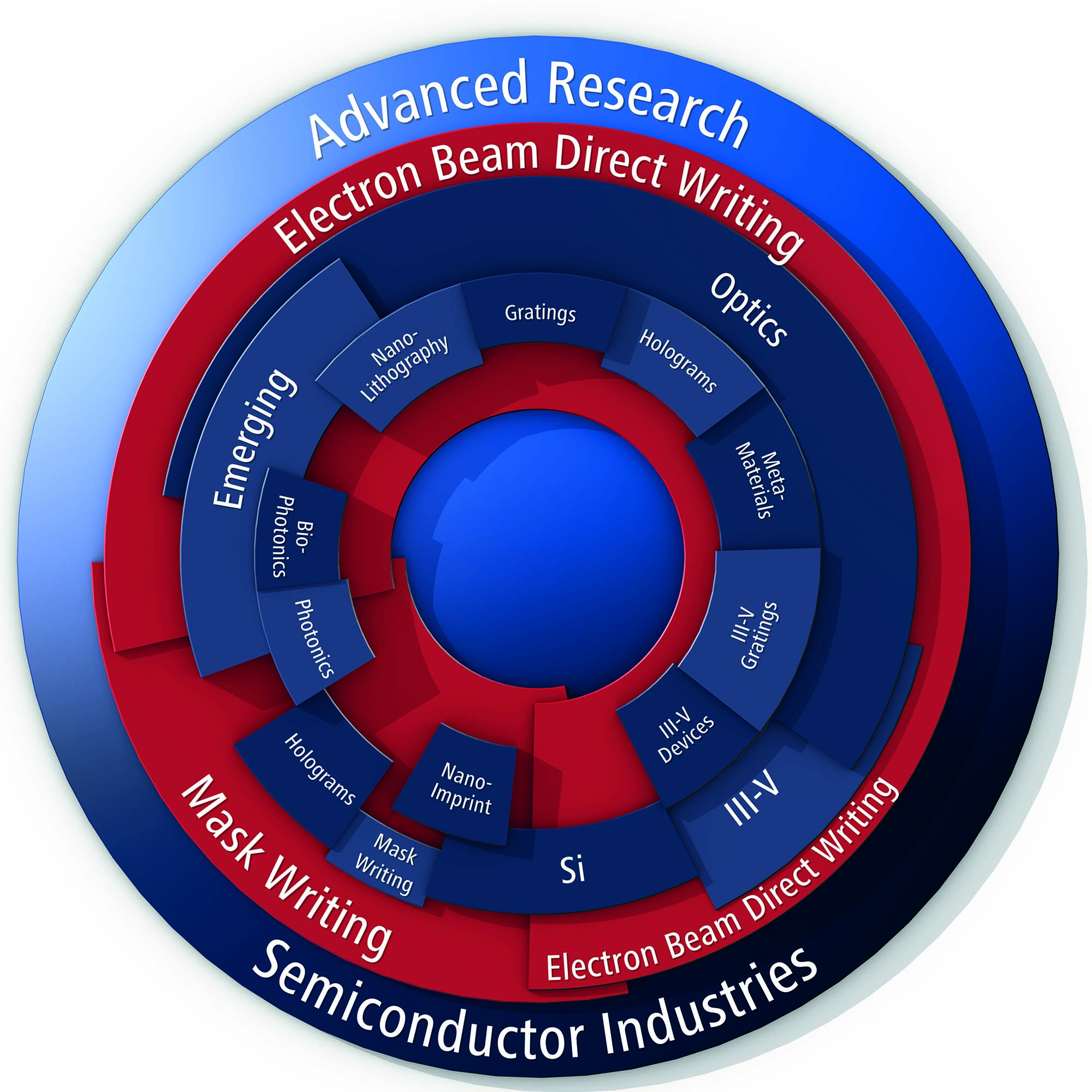
Vistec Product Portfolio
As a long-standing equipment supplier, Vistec Electron Beam GmbH, Jena (Germany) is providing leading technology solutions for advanced electron-beam lithography. Based on the Variable Shaped Beam (VSB) principle, the electron-beam lithography systems are mainly utilized for semiconductor applications and advanced research as electron-beam direct write in semiconductor manufacturing, mask making as well as integrated optics and several new emerging markets.
Vistec Electron Beam´s roots go back to the 1950´s when the company was part of Carl Zeiss Jena where the first electron microscope was developed. In 1974, the first commercial shaped beam system was launched on the basis of fundamental patents.
In addition to its production facility in Germany, Vistec Electron Beam maintains service and support centers in Europe, Taiwan and in the US.
The Vistec SB254 electron beam lithography system has been designed as a universal and cost-effective tool for both direct write and mask making applications to allow the customers to react quickly to market demands. With its 210 x 210mm stage travel range it is the ideal tool for exposing masks up to 7inch and wafers up to 200mm diameter. The concept of the SB254 enables handling and exposure of transparent and non-transparent compound semiconductor materials. The modular system architecture allows your SB254 to be adapted to meet your application requirements. The small cleanroom footprint and the fully automated substrate handling as well as the state of the art operating and data preparation software will convince you of the excellence of the SB254 Series being part of the modular toolset Vistec is offering to its customers from the industry and applied research sector.
The Vistec SB3050-2 is designed to meet the challenges of direct patterning below the 32 nm technology node, it features Variable Shape Beam (VSB) technology with vector scan and continuously moving stage principles for throughput optimization. Our industry proven 300 mm design concept has been successfully utilized in several installations worldwide. The Vistec SB3050-2 combines state of the art substrate handling with a high-precision stage system and a sophisticated electron-optical 50 keV column specifically developed to ensure excellent resolution performance.