Company type
Home | Mitglieder |
AP&S International GmbH
Medium-sized companies (<250 employees or <50 million annual turnover)
Target markets
Electronics·Life science·Machinery and Equipment·Public Sector
Industries
Machinery & Equipment·Technology
Portfolio
batch- and single wafer wet process equipment·eless plating·Equipment·Micro- / Nanoelektronics·other·parts cleaning equipment·Semiconductor Industry
Certificates
Contact
Obere Wiesen 9
78166 Donaueschingen
78166 Donaueschingen
0771 8983-0
Contact Person
Patrick Hirt
+49 351 8925 - 129
Vice President Business Development

About this member
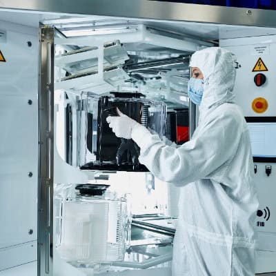
AP&S – WE ARE YOUR PARTNER FOR WET PROCESS EQUIPMENT
For over 20 years, we have been supplying high-performance wet process equipment for the surface treatment of wafers to the world's leading semiconductor manufacturers. Our modular product range is perfectly tailored to the needs of the semiconductor industry, whether standard wet process equipment or a customized solution is required.
AP&S is a global specialist in the development and construction of wet process equipment used in the manufacture of microelectronic chips. Our customer base includes renowned companies from the semiconductor industry, optoelectronics and sensor technology.
Batch Processes
NexAStep, TeraStep, A-Series, Vulcanio, GigaStep, MultiStep, TwinStep, NID Dryer
High throughput, optimized process operating costs, comprehensive process control and consistent process results for vertical wafer processing.
The main feature of batch processes for the production of semiconductor devices and microelectromechanical systems (MEMS) is the simultaneous processing of multiple wafers on the front and back side. AP&S’ batch wet process portfolio includes simple manual wet benches for laboratory or R&D purposes as well as fully automated high-end technology wet benches for mass production. Bridge tools for flexible wafer sizes are our strength! Due to the perfectly coordinated interaction of product design, automation and the required chemicals, our wet process solutions for batch processing offer maximum process reliability, optimized process times, cost efficiency and maximum flexibility.
AP&S’s wet benches enable cleaning, drying, etching, PR stripping and electroless deposition (e-less plating) for wafer processing up to 12 inches and masks of various sizes.
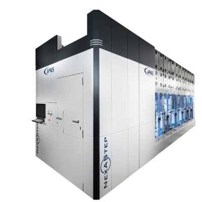
AP&S NexAStep
Single Wafer Processes
SpinStep Flexline, SpinEtcher, SpinLift-off, SpinMask, SpinMetal, SponRCA, SpinScrubber, Mini Chemical Management System
High-precision processes with high uniformity, high repeatability and extremely precise process control for horizontal wafer processing.
AP&S’ single wafer processing portfolio includes a variety of processes for the semiconductor and MEMS production chain: cleaning, drying, etching, metal etching, photoresist (PR) stripping and metal lift-off processes. The in-house AP&S laboratory “DemoCenter” offers you a wide range of demonstrations with the single wafer tool.
Our horizontal wafer handling machines can handle all standard substrate formats: 100 mm, 125 mm, 150 mm, 200 mm and 300 mm. Thereby, we cover all common substrate materials and substrate thicknesses in semiconductor production.
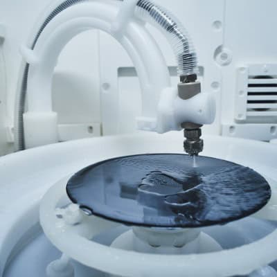
AP&S Single Wafer Processing
Produktionsunterstützendes Equipment
CleanSurF, CleanStep CBII & CBIII, SprayCleaner, CleanStep Tube, Chemical Management Systems
FOUP, SMIF, carrier and box cleaners, wafer drying equipment and chemical management systems are also part of our portfolio.
Our primary goal is to ensure efficient wet processes in our customers’ semiconductor fabs. Therefore, our product range also includes fab logistics equipment such as FOUP and box cleaners, drying units for wafers, cleaning systems for quartz tubes, liners and boats, and chemical management systems.
In this way, our customers receive everything from a single source and have a competent partner at their side for all relevant issues relating to wet-chemical processes in their semiconductor production.
AP&S C