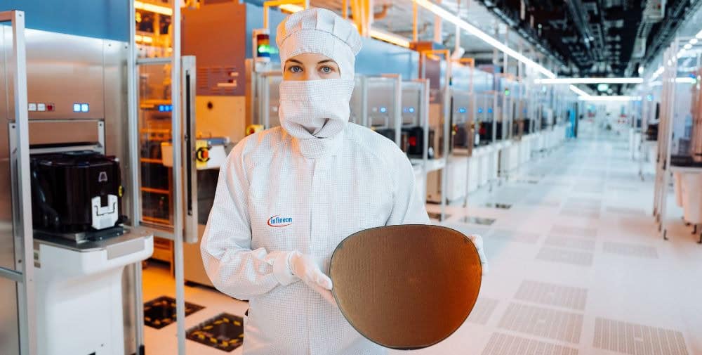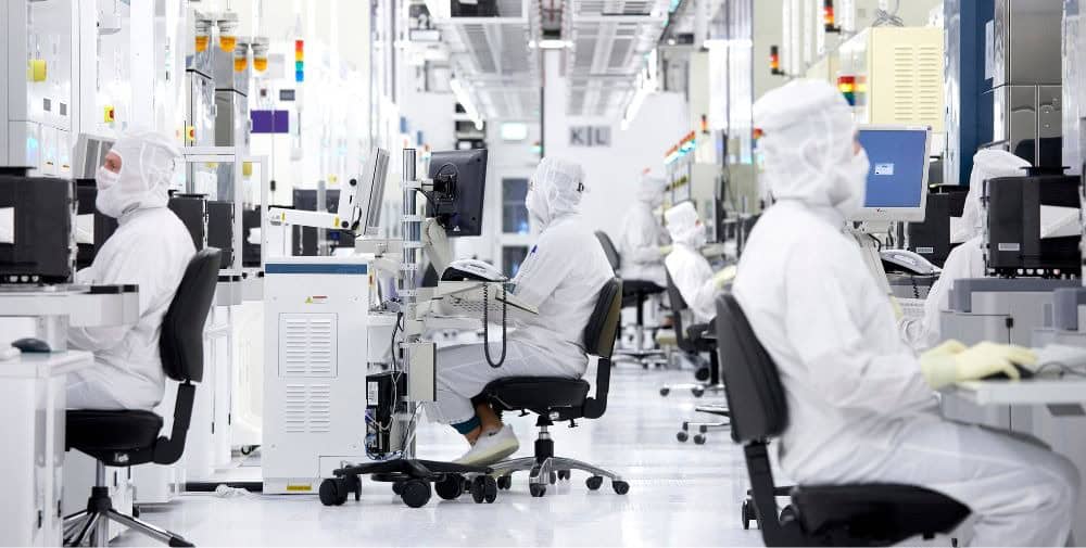
“The world’s thinnest silicon wafers are proof that we at Infineon are pushing the technical boundaries of power semiconductor technology to the limit to deliver world-class value to our customers,” said Jochen Hanebeck, CEO of Infineon Technologies. “Infineon’s breakthrough in ultra-thin wafer technology is a significant step forward in energy-efficient power solutions and helps us to realize the full potential of the global trends of decarbonization and digitalization. With this technological masterpiece, we are consolidating our position as an innovation leader in the industry by mastering all three relevant semiconductor materials with Si, SiC and GaN.”
The innovation will help to significantly increase energy efficiency, power density and reliability in power supply solutions for AI data centers, consumer, motor control and computing applications. Halving the wafer thickness reduces substrate resistance by 50 percent. Power losses in power systems can thus be reduced by more than 15 percent compared to solutions based on conventional silicon wafers with a thickness of 40-60 micrometers. This is particularly important for the power supply of advanced AI server applications, where the increasing demand for energy is driven by higher current levels. In AI data centers, voltages of 230 V must be reduced to a processor voltage of less than 1.8 V. Ultra-thin wafer technology promotes a vertical power supply design based on trench MOSFET technology that enables very close positioning to the AI chip processor, reducing power losses and improving overall efficiency.
“The new ultra-thin wafer technology fuels our ambition to power diverse AI server configurations in the most energy-efficient way, from the power grid to the processor core,” said Adam White, Division President Power & Sensor Systems at Infineon. “As the power requirements for AI data centers are rapidly increasing, energy efficiency is becoming more and more important. This is a fast-growing business area for Infineon. We expect our AI business to reach a volume of one billion euros in the next two years.”
In order to overcome the technical hurdles of reducing the wafer thickness to 20 microns, Infineon engineers had to develop an innovative and unique wafer grinding approach, as the metal package that holds the chip on the wafer is thicker than 20 microns. This significantly affects the handling and processing of the backside of the wafer. In addition, challenges such as wafer bow and wafer separation have a major impact on the back-end assembly processes that ensure wafer stability and first-class robustness. The thin wafer process to 20 microns is based on Infineon’s existing manufacturing expertise and ensures a seamless integration of the new technology into existing high-volume silicon production lines. There are no additional manufacturing costs to guarantee highest production yields and supply reliability.
Infineon has already qualified the technology with customers and applied it to its Integrated Smart Power Stages (DC-DC converters). Infineon’s innovation leadership in semiconductor manufacturing is underlined by a strong patent portfolio in the field of 20-micrometer wafer technology. Infineon plans to increase the production of ultra-thin wafers and replace existing conventional silicon wafers for low-voltage power supplies with the 20-micrometer process within the next three to four years. This breakthrough strengthens Infineon’s unique position in the market with the broadest product and technology portfolio encompassing silicon, silicon carbide and gallium nitride-based devices, which are a key building block for decarbonization and digitalization.
About Infineon
Infineon Technologies AG is a leading global semiconductor manufacturer for power systems and IoT. With its products and solutions, Infineon is driving decarbonization and digitalization. The company employs around 58,600 people worldwide and generated revenue of around €16.3 billion in the 2023 fiscal year (ending September 30).
– – – – –
Further links
👉 www.infineon.com
Photo: Infineon


