In recent years, the discussion about disrupted value chains has focused strongly on missing chips for the automotive and electronics industries. Rather little public attention was paid to what a sophisticated high-tech product the microelectronic circuit is and what complex paths lead from sand to chip. It is all the more remarkable that most semiconductor manufacturers continue to successfully keep their own value streams flowing, regardless of all the global crises.
This task is demanding: to manufacture a microelectronic circuit, you need high-purity silicon, targets for the ion implanters, noble gases, aqua regia and many other chemicals, multi-million dollar facilities, know-how accumulated over decades, and an excellent system to coordinate thousands of people and process steps around the globe. De-globalization in the semiconductor industry? Difficult, because no single country is able to fully realize all links of the semiconductor value chain within its own borders. Some chips circle the globe two and a half times from sand to assembly at the end customer.
From sand to chip – a quick run
As a reminder, here is an overview of a typical semiconductor process chain: The starting material is often quartz sand. The raw materials industry reduces this silicon oxide to silicon in electric furnaces at temperatures of around 2000 degrees Celsius and delivers it to specialized chemical companies such as “Wacker” with a purity level of around 98 percent. There, fluidized bed reactors turn it into the gas trichlorosilane, which can be further purified very well in distillation plants. The hyperpure silicon is then separated from this in special reactors at around 1100 degrees.
Grown giant crystal cut into slices
From this initially still disordered polysilicon, companies such as “Siltronic” then use a seed crystal to grow a single crystal called an “ingot,” which is about two meters long. This is cut into slices called “wafers” with a diamond saw, ground, cleaned and, in some cases, already epitaxied, i.e. provided with an additional surface crystal layer.
Like a sandwich: layer structure in the chip factory
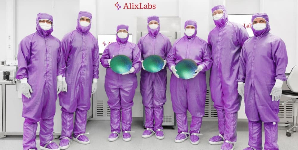
Chip factories such as those of Infineon, GlobalFoundries, Bosch or X-FAB then process the wafers further in clean rooms in which there are no dust grains, skin particles or other tiny foreign bodies. For this reason, chip workers are only allowed to enter these clean rooms when wearing appropriate protective clothing. In the clean room, machines further coat the wafers and then cover them with photoresist. Lithography systems expose these coatings in the following with the aid of special light sources and masks that contain the circuit design of each individual chip level. In this way, the future chip structures are burned onto the resist – at first temporarily. These structural images are then etched away and the wafers are bombarded with foreign atoms (ions) that have previously been removed from so-called “targets. This creates conductive tracks and components at the desired locations. The systems repeat these process steps until all circuit layers have been created and interconnected.
With the help of the automatic transport system, the wafers travel from station to station in boxes. The wafer boxes themselves often contain nitrogen to prevent undesirable reactions of the wafers with the air. Low-reactivity inert gases such as neon are also needed for some process steps, including to power certain lasers.
Journey to Asia in the backend factory
Once the wafers have been processed, i.e. once the functionalities of the desired processors, memories or other chips have been implemented on them, the so-called “front end” is complete. Now the “back end” begins: In most cases, these wafers are airfreighted to specialized factories in Asia. There, machines cut the wafers into individual chips, fit them with plastic or ceramic housings and equip them with electrical contacts to establish the signal paths between the chip and the “outside world. Finally, the circuits are returned to test centers or to the “home companies,” some of which may be located in Europe or North America.
Of course, all this is only a rough overview. In fact, many other value chains are involved in chip production. These include, for example, the development and production of the often very expensive manufacturing equipment, circuit design and the entire supply chains with electricity, heat, cooling, process gases, implantation material and the like. Keeping these chains and flows functional was and is a challenging task for semiconductor companies, one they have mastered impressively even in past times of crisis.
Multi-source approach expanded
GlobalFoundries Dresden, for example, has recently increased the proportion of supply lines in which not just one but two or more sources are capable of delivering, reports factory boss Manfred Horstmann. The aim of this multi-source approach is to obtain as many process gases, doping blanks (targets), equipment parts and other items as possible from more than one partner or more than one region of the world. In principle, this is not a new idea, but one that had lost importance in the meantime.
“However, this is not possible in every case,” explains Marek Jakowatz of the Bosch factory in Dresden, who was responsible for global supply logistics in the Bosch Group for many years. “For some supplies, there is only one source – at least at affordable prices.” After all, for some equipment or special materials, there is just one supplier worldwide. There are also highly specialized products whose manufacture is only worthwhile if a supplier also receives sufficient orders for them. Often, the semiconductor companies deliberately distribute the orders for such inputs in such a way that two or more suppliers can actually make a living from them. In other cases, the alternative sources do not meet the semiconductor industry’s quality criteria. “Then it can make sense to continue the qualification process in spite of everything, so that you can fall back on this source in the event of a crisis,” Jakowatz says. The semiconductor experts thus prepare the use of an alternative product in the long term, but then only pull this “joker” in times of crisis. Because: “Something like this needs to be prepared for the long term.”
The view at GlobalFoundries is similar: “Every supply product, especially in the chemical sector, should not be a “single source”, but should have one or two alternative sources,” emphasizes Yvonne Keil, who is responsible for securing the material supply chains at GlobalFoundries. To this end, she says, the company has since diversified its supply base through new supplier qualifications.
More warehousing and recycling
In addition, many Saxon semiconductor factories have been expanding their warehousing for some time, increasing their recycling capacities, installing solar cells for an additional in-house energy supply, and exchanging missing material with other company sites in the event of bottlenecks. Many high-tech companies are also expanding their monitoring systems, which they use to monitor supplier flows. In the meantime, it is necessary to keep an eye not only on the company’s own suppliers, but also on the suppliers’ suppliers, reports Manfred Horstmann. To do this, special software evaluates seven days a week and around the clock what impact unforeseen events have on the supply chains and what the procurement situation is like for each location and material at any given time, explains Yvonne Keil.
A few supply streams at a glance
Here now are a few examples of the material and product chains that require a lot of organizational talent in modern chip factories:
Gases and chemicals
In a way, you can think of a chip factory as a chemical plant with a semiconductor plant on top. Chemicals and especially gases that are essential for circuit production include aqua regia, neon, argon, helium, nitrogen, oxygen and hydrogen. In some cases, chip companies procure these substances locally or regionally, for example from Leuna, but some can only be obtained internationally.
For example, the chemists use aqua regia to dissolve gold for etching chemistry in the clean room. In turn, the plants need some of the gases mentioned as low-reactivity inert gases, as chemicals for certain process steps or for the oxidation of production residues. Noble gases such as neon are needed by companies that do not use extreme ultraviolet (EUV) equipment for argon fluoride lasers, which serve as 193-nanometer light sources in traditional lithography. And nitrogen protects the wafers from contact with air – allowing wafer transport carts to bridge longer waiting pauses in front of crowded production stations. Bosch Dresden, for example, separates this nitrogen from the air under high pressure using its own decomposition system. The company therefore only needs to buy in this gas when demand is high.
Neon, on the other hand, recently threatened to become scarce at times because Ukraine, the main global source, was hardly able to deliver after the Russian attack. Meanwhile, distributors have diversified their neon supply chains and chip factories have increased their neon inventories. In addition – and this applies to all chemicals and process gases – recycling is playing a growing role. There are often special “chemistry cabinets” for this purpose in the subfabs under the clean room, some of which are operated by external specialist companies.
Wafer
Depending on the plant park and specific orders, some chip plants need 200-millimeter wafers, others 300-mm wafers, which then sometimes consist only of pure silicon or are already pre-coated, i.e. epitaxied (“epi-wafer”). The Saxon semiconductor factories purchase a large proportion of their wafers from European and, in some cases, German manufacturers who have committed themselves to long-term contracts. Bosch has already announced its intention to increase the share of European wafers in the near future.
Equipment
For their equipment pool, microelectronics companies usually tender their orders right away so that basically up to two to four suppliers should be able to deliver. Some key equipment suppliers like ASML are located in Europe, but others are located in Japan, in the USA and in other countries. Therefore, global transport chains must always be organized for the equipment or for equipment repeat orders. It is also important to ensure a highly available maintenance service for the machinery.
There is also the issue of capacity utilization. Currently, for example, delivery times are very long in some cases.Because of the chip bottlenecks in recent years, semiconductor groups such as TSMC, Intel, GlobalfoundriesGlobalFoundries, Infineon and Bosch are therefore gradually expanding their capacities, which in turn means that many equipment manufacturers are overbooked for the long term. “Everyone is ordering like crazy,” reports Bosch manager Marek Jakowatz. Despite the recent gloom in the economic skies, many still expect demand for microelectronics to remain strong, especially for automotive electronics – with the corresponding cascading effects down to the equipment suppliers. In other words, long equipment delivery times are likely to continue for the time being.
Spare parts
For spare parts replenishment, many companies are relying on stronger supply chain monitoring and more warehousing than in the past. Here, the chains to be stabilized are often particularly “tricky”: sometimes only a very specific plastic granulate is missing for an injection molding factory, which in turn supplies plastic tubes for a semiconductor machine. In the worst case, such a triviality stops an entire production line in a chip factory or slows down new equipment.
Water
Currently, the water supply for the semiconductor industry in and around Dresden is considered stable and secure. However, in view of the expansion plans of the existing fabs and possible new settlements, it is foreseeable that the industrial water demand in the Elbe Valley will still increase significantly. Many factories are therefore increasingly investing in their own ultra-pure water treatment and water recycling plants. In the long term, however, a larger solution is needed. To this end, “Sachsenenergie” designed a long-term supply concept for the Dresden semiconductor industry and related sectors in consultation with the city, the Free State and the business community. This is currently being implemented at full speed.
Transport
The Saxon semiconductor industry already uses many different transport routes for its supplies: Wafers arrive by truck, plane or ship, for example.
Gases and chemicals usually reach the chip factories by tanker trucks. Alternatively, the fabs have sometimes built their own pipeline systems. For some substances, environmentally harmful transports are not necessary if the factories separate them from the air themselves, as is the case with nitrogen.
There are also efforts to organize transports by rail, for example via the “New Silk Road”. But since the envisaged rail lines from Asia to Europe run through Russia, this project has been put on hold since the attack on Ukraine.
“Transport route resilience” has in any case become very important for Bosch, GlobalFoundries, and other players at the site. Because experience has shown that customers with large order volumes receive preferential treatment from suppliers in the event of production, transportation and other bottlenecks, there are discussions about whether shared warehouses or logistics organizations could give the Saxon semiconductor industry an advantage on this point.
Backend
In addition to material flows to their own front-end clean room, chip factories also need to at least keep an eye on downstream back-end process chains all the way to the finished circuit. Bosch Dresden, for example, delivers some of its finished processed wafers unbroken to other fabs within the group or to external customers. Although the Saxon plant does not have a complete backend, it at least has its own capacity to cut wafers as needed and separate them onto foils. The typical case, however, for the Bosch fab as well as most chip plants in the Dresden area is the transport of complete wafers to assembly factories in Asia. Because fully processed wafers often already represent the equivalent value of a home and the old motto “time is money” applies here, fast transport as air freight is common for these value-intensive goods. The subsequent tests then also take place partly in Asia, but partly again in Europe. When air cargo capacity constraints arise, larger players sometimes charter their own aircraft.
Energy
Many Dresden chip factories have now stepped up their efforts to save electricity and heating costs, as well as to make their energy supply more secure and self-sufficient – and often more environmentally friendly as a “side effect.” For example, GlobalFoundries has installed redundant access points to the 110-kilovolt power grid, and replaced old lights with energy-saving LEDs in many places. The chip plant also has diesel-powered heating boilers and can run some equipment on propane. In 2023, a solar system on the factory roof went into operation and has since covered about five percent of the site’s electricity needs. In addition, starting in 2025, factory manager Horstmann plans to cover about 20 percent of the current natural gas demand with purchased hydrogen. “We have enough backup solutions to keep the factory running at all times,” he assures.
Similar approaches are being taken by Bosch in Dresden, where the setup team has installed a diesel-powered emergency power supply and a battery-based “uninterruptible power supply” (UPS). Together, the two can bridge small power outages. And in the event of longer power outages, they at least make it possible to keep particularly important equipment running for half an hour to an hour and to shut down the machinery in an orderly fashion. The Bosch factory in Dresden is also planning a photovoltaic system and the supply of hydrogen or liquid gas. Whether the fab will produce the hydrogen itself on the factory premises or use Bosch fuel cells to generate energy – all these and other questions have not yet been conclusively clarified.
This article was first published as part of our NEXT magazine “In Focus: Microelectronics”.
👉 Go to the complete issue of the magazine
Photo: Shutterstock


