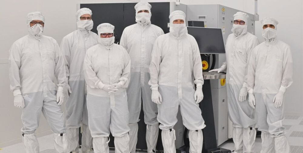
To kick off this extended collaboration, Fraunhofer IZM-ASSID has acquired a fully automated EVG®850 DB UV laser debonding and cleaning system and installed it at Fraunhofer’s newly founded Center for Advanced CMOS and Heterointegration Saxony (CEASAX) in Dresden. CEASAX combines the core competencies of Fraunhofer IZM-ASSID and the Fraunhofer Institute for Photonic Microsystems (IPMS) to advance research in the field of 3D / heterogeneous system integration at 300mm wafer level and front-end semiconductor integration processes for high performance neuromorphic computing, cryo and quantum technologies.
The EVG850 DB is the first system ever to be installed at CEASAX. It will help Fraunhofer IZM-ASSID to close critical process gaps and provide technology modules for the fabrication of quantum systems and their wafer-level hardware environment in a 300 mm wafer cleanroom environment. The installation of the system also marks the launch of the Fraunhofer bonding hub, which will also include a variety of state-of-the-art temporary and permanent wafer-to-wafer and die-to-wafer bonding systems.
Temporary bonding: essential for heterogeneous integration applications
Temporary wafer bonding is a widely used method to enable the processing of thin wafers (less than 100 micrometers silicon thickness) required for 3D ICs, power devices and fan-out wafer-level packaging (FOWLP), as well as the processing of sensitive substrates such as compound semiconductors. Deboning the carrier wafer is an essential step in preparing the product wafer for the final process steps of separating and integrating the chips or dies into the final product or application. With the acquisition of the EVG850 DB system, Fraunhofer can carry out these debonding processes entirely in its own clean room, which enables significantly shorter development times for optimal process sequences with different bonding material systems. This in turn enables Fraunhofer to optimally adapt its processes to the individual and specific needs of its numerous customers.
“Fraunhofer and EV Group have a long and successful history of collaboration in developing new processes that have enabled groundbreaking new microelectronics applications – including the multi-device integration of analog and digital devices such as ASICs, RF devices, sensors and transceivers into an optimized system-in-package or functional, intelligent microelectronic systems,” said Manuela Junghähnel, Site Director of Fraunhofer IZM-ASSID. “We are pleased to expand and strengthen this partnership with the purchase of the EVG850 DB laser debonding and cleaning system. The system will be the first of several major product installations at CEASAX, our new and advanced semiconductor research center. This expanded partnership brings state-of-the-art technology in-house for Fraunhofer and provides EV Group with a strong partner for the development of new technologies for 3D device integration, which in turn offers our customers an even more end-to-end process chain for 3D / heterogeneous integration from a single source.”
Markus Wimplinger, Corporate Technology Development and IP Director at EV Group, said: “We are delighted to extend our long-standing partnership with Fraunhofer to applications in quantum computing and beyond through this latest strategic development. Our expanded collaboration allows EVG to remain at the forefront of technological advancement and enables us to contribute to the development of new manufacturing processes for quantum systems.”
EVG Solutions for Heterogeneous Integration
EVG’s wafer bonder, lithography and metrology solutions enable the development and high-volume manufacturing of technology innovations in advanced packaging – including backside exposed CMOS image sensors and other stacked 3D ICs – as well as in MEMS and compound semiconductors. Recent breakthroughs in hybrid bonding to meet the requirements for 3D integration of devices, wafer bond alignment for future 3D IC packaging requirements, IR laser release technology to replace glass substrates in advanced packaging and 3D stacking of ultra-thin films, maskless exposure for fan-out wafer-level packaging (FOWLP), NIL applications and resist processing for the production of wafer-level optics (WLO) are just a few examples of EVG’s technological leadership in the fields of heterogeneous integration and wafer-level packaging.
About the EVG850 DB System
The fully automated EVG®850 DB UV laser debonding and cleaning system enables room temperature debonding of ultra-thin and stacked fan-out packages with high throughput and low cost of ownership. The system uses a solid-state UV laser and proprietary beam shaping optics to enable optimized carrier lift-off without force. For more information about the EVG850 DB UV laser debonding and cleaning system, please visit www.evgroup.com/de/products/bonding/temporary-bonding-and-debonding-systems/evg850-db.
About Fraunhofer IZM-ASSID
Fraunhofer IZM-ASSID (All Silicon System Integration Dresden) develops leading wafer-level packaging and system integration technologies for 3D integration through silicon vias (TSVs) and converts them into products. It has a complete 300mm process line for TSV formation and the realization of 3D assemblies. Fraunhofer IZM-ASSID’s range of services includes customer-specific developments, prototyping and series production in small quantities as well as technological process transfer.
About EV Group (EVG)
EV Group (EVG) is a recognized technology and market leader for precision equipment and process solutions for wafer processing in the semiconductor industry, microsystems technology and nanotechnology. Its core products include wafer bonders, thin wafer processing systems, lithography and nano-bead lithography systems as well as photoresist coaters, cleaning and metrology systems. Founded in 1980 and headquartered in St. Florian am Inn (Austria), the company employs more than 1,300 people and serves well-known production customers and R&D partners around the world with its own subsidiaries in the USA, Japan, Korea, China, Taiwan and Malaysia as well as representative offices. More information is available at
– – – – – –
Further links
👉 www.izm.fraunhofer.de
👉 www.EVGroup.com
Photo: Fraunhofer IZM | Silvia Wolf