High-performance and supercomputers are of enormous importance for an efficient digital future and technological sovereignty. In high-performance computing (HPC), data centers collect huge amounts of data and use it to perform complex calculations. HPC is therefore used wherever computationally intensive operations are required at high speed: This benefits science in particular for creating complex simulations and algorithms, but supercomputers are also already being used to optimize transport, logistics, industry and precision medicine. HPC is just one of many promising applications that are based on performance and efficiency.
New connection technologies are crucial to meeting these high requirements. The idea behind this is that the smaller the pitch, i.e. the distance between electronic contact points, the more transistors and circuits can be accommodated on a chip, which in turn leads to higher performance. Until now, copper bumps with solder have proven to be the standard technology for flip-chip applications. With increasing miniaturization, however, this process is reaching its limits, as the solder material can leak out and lead to short circuits.
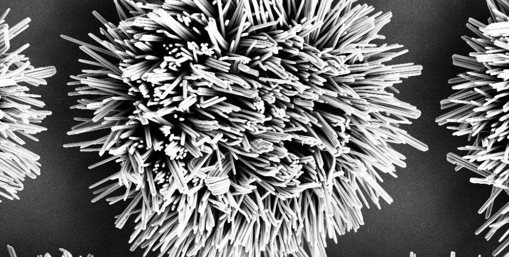
In order to find innovative alternatives, Jun.-Prof. Dr.-Ing. Iuliana Panchenko and her team at Fraunhofer IZM-ASSID are researching new connection technologies for small contacts of less than 10 micrometers. As part of the Fraunhofer-funded SME project “NanoInt”, the team developed a promising solution with copper nanowires together with partners from science and industry and successfully evaluated the process for application on 300 millimeter wide silicon wafers.
In comparison to other approaches such as soldering with copper or solder bumps, hybrid or compression bonding, the direct copper connection with nanowires offers several advantages. Thanks to the plug-in principle (nanowire-to-nanowire), this connection technology tolerates more height variations, requires no additional metals, offers more design freedom and ensures good mechanical strength. In addition, contacting can be achieved at room temperature and with low bonding pressure. This means that the resource-saving technology is also suitable for low-temperature bonding and therefore for temperature-sensitive and thin chips.
In the first phase of the project, the focus was on achieving the most homogeneous possible growth of nanowires at the connection points across the entire 300 mm wafer. The research team used membranes with fine pores for this purpose. The pore diameter is decisive for the thickness of the nanowires and can be varied between 100 nm and 1 µm. In order to create conductive and reliable connections, the pore density had to be evaluated in advance. In an electroplating process, the copper nanowires grow in the pores of the membrane. By optimizing the process, a variation in nanowire heights of around 20 percent was achieved across the entire wafer. In addition, the research team has developed a process sequence that protects the nanowires during the etching processes so that the conductive copper seed layer on the wafer can be removed.
In order to evaluate the bonding technology close to the application, the researchers demonstrated the integration of the process into the industrial processing chain. For this purpose, the optimal parameters for the further assembly of such structures were identified and implemented with special attention to reproducibility, homogeneity, mechanical strength and industrial suitability.
At the end of the project, the partners demonstrated a 300 mm silicon wafer with uniform nanowires as bumps and a chip-to-chip structure with nanowire connections. This demonstrates successful system integration for 2.5D and 3D assemblies without the use of fluxes. As a result, the technology is already being offered to industry. In upcoming research projects, the contacts are even expected to shrink from 10 to less than 5 micrometers. In the future, the application areas of the nanowire connection technology can be expanded so that it can be used for complex packages with fine pitch and large-area contacts.
Other partners in the NanoInt project are NanoWired GmbH, Fraunhofer IMWS and IAVT at TU Dresden.
– – – – – –
Further links
👉 www.izm.fraunhofer.de
Photo: Fraunhofer IZM