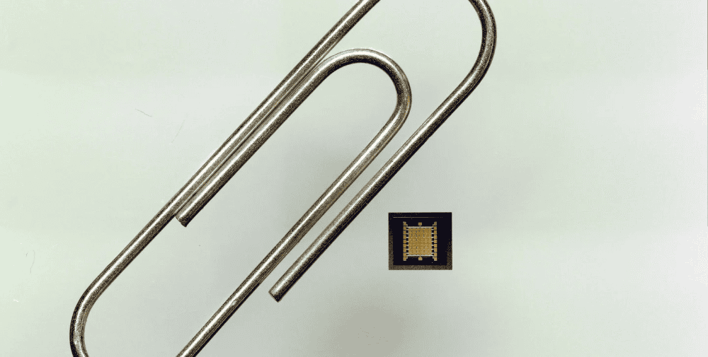
The Fraunhofer Institute for Photonic Microsystems IPMS has completed the collaborative project “MEMS-Based Parametric Amplifiers for Range Optimization of Wireless Sensor Networks” (MEMS-ParAmps) in collaboration with the Hamburg University of Technology (TUHH) and Actemium BEA, an application partner based in Lusatia. The project developed a generic, energy-efficient platform for battery-powered monitoring applications that combines a wake-up receiver with a novel parametric MEMS amplifier. The project ran from October 1, 2021, to January 16, 2026.
Starting Point and Objectives
Wake-up receivers keep sensor nodes permanently ready to receive signals without activating the main electronics, and require very little energy to do so. However, their reception sensitivity is significantly limited, which restricts the achievable wireless range. The project consortium therefore adopted the approach of connecting a parametric MEMS amplifier in series with the receiver. The team defined target values of a battery life of up to ten years and a range of up to one kilometer in open space.
“Until now, one had to choose between long range and long battery life. With our new amplifier chip, it is possible to combine both,” explains Dr. Michael Stolz, project manager at Fraunhofer IPMS.
Technical Results
The project covered the entire development chain, from system specification through the design and fabrication of a novel micromechanically tunable capacitor (MEMS varactor), including the associated drive circuit. A key focus was on an energy-efficient voltage pulse generator that enables the mechanical excitation of the varactor with approximately 3.3 microjoules per pulse. This corresponds to a tiny fraction of the energy of an LED lamp. Since commercial measurement systems did not meet the requirements, the project partners also developed their own methodology for dynamic capacitance measurement with a bandwidth of over 10 megahertz to verify the component’s function.
Protocol Adaptation and Validation
To ensure the technology works in practice, the team adapted an existing wireless communication protocol for long distances between the sensors. Together with the industry partner Actemium BEA, the subsystems were tested in a simulated laboratory scenario. The central communication platform, consisting of an energy-efficient microcontroller and a radio transceiver, was also set up and successfully tested. This demonstrates the fundamental feasibility of the solution at the theoretical and simulation levels.
“Adapting the protocol to large distances between nodes was just as crucial as the hardware itself. Validation in the laboratory scenario has shown that the concept can be adapted to the constraints of industrial applications,” said Prof. Dr. Alexander Kölpin, project leader at the Technical University of Hamburg.
Application Prospects and Establishment in Lusatia
The developed MEMS components and circuit concepts can be used, among other things, in low-noise mixers, highly sensitive wake-up receivers, and energy-autonomous sensor nodes. A demonstrator has already been presented at Sensor+Test in Nuremberg (2022, 2023, and 2025) as well as at ICCC2024 in Cottbus. The demonstrator was also on display in September 2024 at the Science Gallery of the Cottbus Innovation Center (IKMZ). The fact that the technology is already gaining a foothold in Lusatia is further evidenced by a bachelor’s thesis submitted as part of the project at BTU Cottbus-Senftenberg.
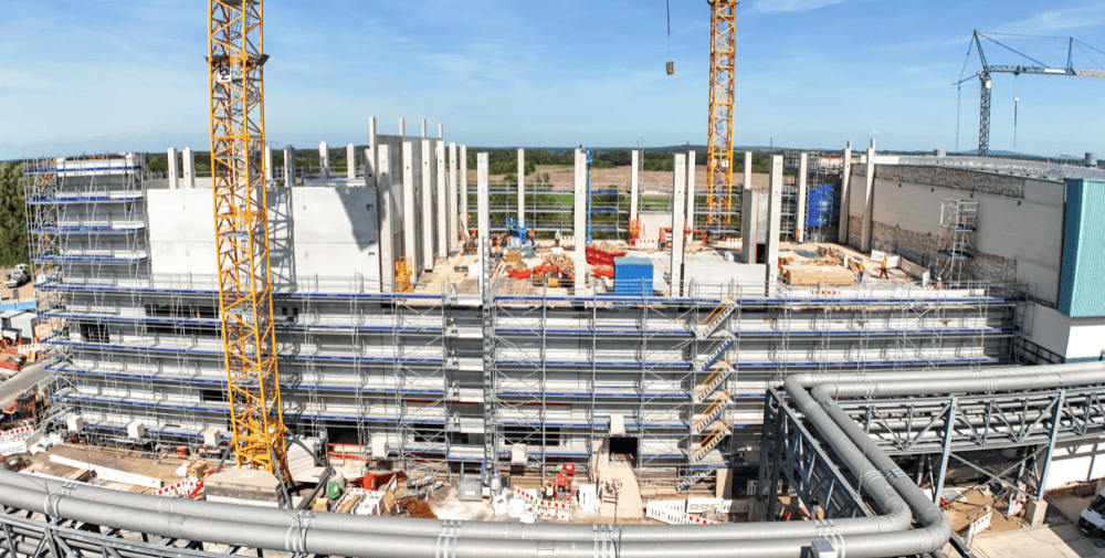
As the project nears completion, the infrastructure in which such developments are to take shape in the future is also growing: Cottbus is increasingly establishing itself as an important Fraunhofer location. On October 1, 2026, the groundbreaking ceremony took place for a new, state-of-the-art office and laboratory building, which is being constructed north of the central campus of BTU Cottbus-Senftenberg as part of the structural transformation of the Lusatia region. In the future, the building will house research groups from Fraunhofer IPMS, specifically the Integrated Silicon Systems (ISS) division, as well as other Fraunhofer Institutes, institutions of the Leibniz Association, and the German Aerospace Center (DLR). Together with the Brandenburg University of Technology Cottbus-Senftenberg, the new building forms a central component of the Lausitz Science Park and strengthens the region as a high-performing research and innovation hub.
“With this new building, we are pooling our expertise in Lusatia and creating laboratory environments to continue developments such as those from MEMS-ParAmps in collaboration with regional partners,” says Dr. Sebastian Meyer, head of the Integrated Silicon Systems (ISS) division at Fraunhofer IPMS.
– – – – –
Related Links
👉 www.ipms.fraunhofer.de
Photo: Fraunhofer IPMS