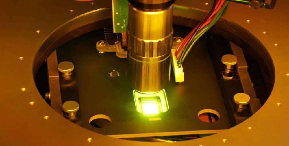
Johannes Zeltner, PhD student at Fraunhofer IPMS, explains: “This outstanding brightness was achieved by stacking OLED layers. The individual OLED units are “connected in series”, which increases the brightness with each additional unit without increasing the current density in the component. This can be used either to achieve extremely high brightness levels or to reduce the current density, which is decisive for the service life of a given brightness level. Measurements have shown that in comparison between a 1-unit and 2-unit OLED, the lifetime LT95, i.e. the drop in brightness by 5%, can be significantly improved from 900 to 1300 hours at 50,000 nits.”
The current efficiency and brightness of 1-, 2- and 3-stacked OLEDs were initially evaluated on passive test substrates and were then successfully transferred to 0.62-inch CMOS backplanes with SXGA resolution. This revealed new challenges for further research: while the distance between the subpixels in conventional OLED displays is often several tens of micrometers, in microdisplays it is only a few hundred nanometers. This can lead to crosstalk between neighboring pixels with thicker layer stacks and multiple stacked OLEDs in microdisplays. Solutions to reduce this crosstalk are in preparation.
In addition, the work has shown that narrow-band emission with high brightness is possible through multiple stacking. Here, the spectral emission can be specifically adapted and enables the use of optical concepts with special requirements, such as waveguides or holographic elements.
The researchers are convinced that the ongoing development towards ever higher brightness and improved lifetimes will secure OLED technology a permanent place in the field of AR applications. Nevertheless, there is a continuous need for research, e.g. on optical crosstalk, improved OLED materials and novel backplane architectures.
The researchers are pleased to be able to offer the results achieved and research services to interested partners worldwide in order to take OLED microdisplay technology to the next level and integrate it into marketable products.
About Fraunhofer IPMS
The Fraunhofer Institute for Photonic Microsystems IPMS is a leader in applied research and development in the fields of photonics, microelectronics and microsystems technology for intelligent industrial solutions, medical technology and mobility. Fraunhofer IPMS works on electronic, mechanical and optical components and their integration into miniaturized devices and systems. Its services range from conceptual design and product development to pilot production in its own laboratories and clean rooms.
– – – – –
Further links
👉 www.ipms.fraunhofer.de
Photo: Fraunhofer IPMS


