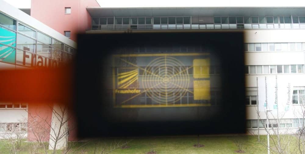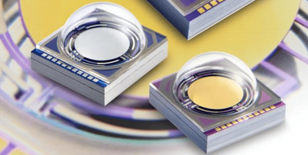
Transparent electronics are already providing reliable services in a number of applications. They can be found as wafer-thin layers for touch displays or as transparent films with printed antennas for mobile communications. However, OLED microdisplays have not been transparent until now.
OlED microdisplays with a transparency of 20% were developed as part of the HOT project (“High-performance transparent and bendable microelectronics for photonic and optical applications”, grant number MAVO 840092) funded by the Fraunhofer Gesellschaft. Now the technology has been further advanced and a transparency of 45% has been demonstrated for the first time in a CMOS OLED microdisplay.
How does this improvement come about?
The OLED-on-silicon technology uses a silicon backplane that contains all the active matrix drive electronics for the pixels. The organic front panel is monolithically integrated on the top metallization layer, which also serves as the control contact for the organic light-emitting diode. The second connection of the OLED is formed by a semi-transparent upper electrode, which is shared by all pixels. The pixel circuit is based on silicon CMOS technology and requires several metal layers to connect the transistors embedded in the substrate. These metal connections are made of aluminum or copper. In addition, the optical structure of the OLED requires a highly reflective bottom electrode to ensure high optical efficiency upwards. These two aspects mean that the pixels themselves are not transparent.
“However, a transparent microdisplay can be realized by a spatially distributed design of this basic pixel structure, creating transparent areas between the pixels as well as minimized column and row wiring,” explains Philipp Wartenberg, Group Leader IC and System Design at Fraunhofer IPMS, “in addition, further optimization of the OLED layers, e.g. by avoiding OLED layers in the transparent areas, introducing anti-reflective coatings and redesigning the wiring helps to further increase transparency.”
There are two basic methods for achieving semi-transparency in optical systems:
- Pixel approach: Here, transparent areas are created between individual pixels.
- Cluster approach: In this method, several pixels are combined to form a larger, non-transparent cluster. Larger transparent areas are created between these clusters.
Both approaches are relevant for different applications in practice. For example, the pixel approach is suitable for image overlay within a complex optical system, where the image is used between other image planes.
The cluster approach is particularly suitable for augmented reality (AR) applications, such as in data glasses, where the pixel clusters are combined into a uniform virtual image using micro-optics above each of the clusters. The transparent areas between the clusters remain unaffected by the optics, allowing a clear view of the real environment.
The technology for transparent microdisplays has been developed to support both techniques. The microdisplay presented at IMID demonstrates the cluster approach with new AR optics.
Optical approach
The optical combination of the individual pixel clusters into a unified virtual image was realized by a microlens array. The optics were designed to enable a close-to-eye setup with a similar distance to the eye as regular corrective eyewear.
About the project HOT
(High-performance transparent and bendable micro-electronics for photonic and optical applications)
This work was funded within an internal Fraunhofer program under grant number MAVO 840092. In addition, the researchers were supported by Fraunhofer IOF in micro-optics.
About Fraunhofer IPMS
The Fraunhofer Institute for Photonic Microsystems IPMS is a leader in applied research and development in the fields of intelligent industrial solutions, medical technology and mobility. Fraunhofer IPMS works on electronic, mechanical and optical components and their integration into miniaturized devices and systems. Its services range from design and product development to pilot production in its own laboratories and clean rooms.
– – – – –
Further links
👉 www.ipms.fraunhofer.de
Photo: Fraunhofer IPMS
