Microdisplays are used in a variety of applications, ranging from consumer electronics to specialized industrial sectors. Here are some of the most important applications:
- Augmented reality (AR) and virtual reality (VR): Enabling immersive experiences in headsets.
- Wearable technologies: Compact and energy-efficient display in glasses, smartwatches and fitness trackers.
- Medical devices: High-resolution image displays in endoscopes and diagnostic instruments.
- Industrial applications: Important information in head-up displays (HUDs) for vehicles.
- Cameras and projectors: compact solutions for digital image display.
- Defense and aviation: display of critical information in cockpits and in helmets.
Thanks to their versatility and compact design, microdisplays are a central component of modern technologies and help to enable innovative solutions in various industries – and the market is growing rapidly.
Fraunhofer IPMS is the only independent research and development center worldwide for microdisplay technologies, which also combines backplane IC design in silicon foundry processes and OLED-on-silicon manufacturing technology in its own clean room under one roof. This enables the institute to develop and manufacture customer and application-specific OLED microdisplays. However, the scientists also develop backplanes for other display technologies, such as micro-LED and LCOS (liquid crystal on silicon).
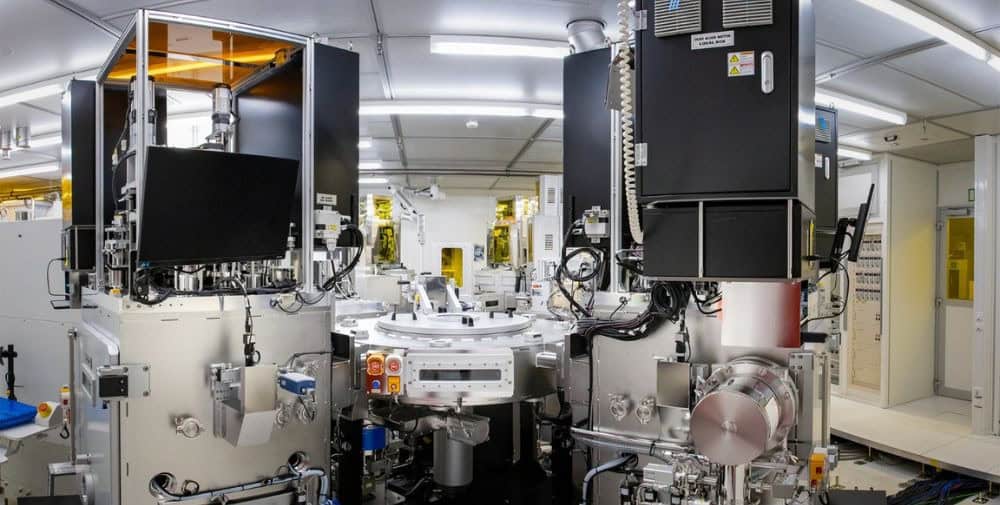
In order to continue to be a leading provider of technology developments in the future, the institute has now expanded and modernized its plant technology. This innovative technology promises a significant improvement in efficiency and quality in the production of high-resolution microdisplays.
“With the new systems, we can thermally deposit complex organic stacks, metal layers and oxides that enable us to develop and produce high-resolution OLED microdisplays, as well as sensors such as organic photodiodes,” explains Bernd Richter, Head of Microdisplay and Sensor Technology at Fraunhofer IPMS. “The industry-compatible systems are state-of-the-art and can be combined so flexibly that they both meet the high requirements of research and development projects and offer high efficiency for pilot production.”
In concrete terms, the new technology achieves a higher throughput and greatly improved process control leads to stable production processes. The system’s new etching chamber is able to carry out various pre-treatments on wafers from different suppliers.
The biggest challenge in this context was to couple the new vacuum system components with the existing system technology.
The scientists are confident that this will enable them to remain competitive in the future and offer their customers a unique portfolio: from the design of microdisplays to the manufacture of initial prototypes and pilot production from a single source.
The acceptance of the new system is planned for the end of October and full operational readiness is targeted by the end of the year. The scientists are convinced that the expanded capacities will enable the institute to remain at the forefront of microdisplay technologies and offer a unique portfolio – from design to manufacturing and pilot production.
– – – – – –
Further links
👉 www.ipms.fraunhofer.de
Photo: Fraunhofer IPMS