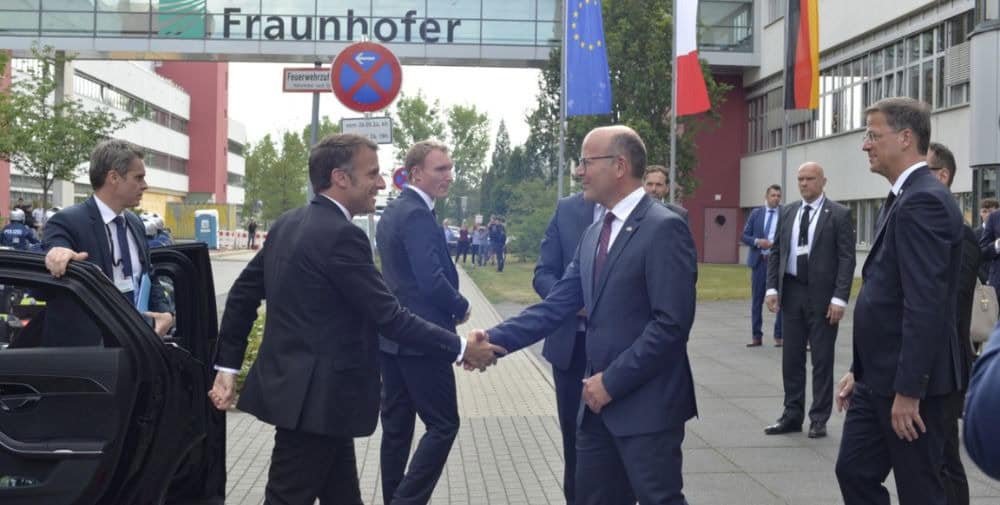
Dresden is one of the most important European locations for the semiconductor industry. And therefore also an important pillar for greater technological independence in Europe. Europe’s sovereignty in technology development is one of Emmanuel Macron’s priorities during his presidency. During his visit, he emphasized how important Franco-German cooperation is for this. It is therefore no coincidence that the only item on the program of the state visit related to technology and science took place in Dresden.
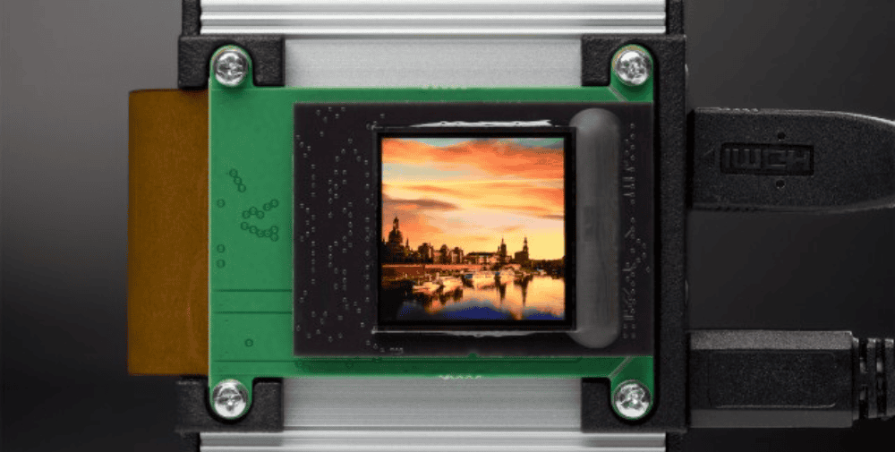
At Fraunhofer IPMS, the two presidents and high-ranking representatives from politics, science and industry had high-tech research in the fields of microelectronics, medical technology and quantum technologies demonstrated to them. Among the high-ranking guests were the French Minister for Higher Education and Research, Sylvie Retailleau, Bettina Stark-Watzinger, German Federal Minister for Education and Research, Jean-Noël Barrot, French State Secretary for European Affairs, Anna Lührmann, Minister of State for Europe and Climate at the Federal Foreign Office and Oliver Schenk, Minister of State for Federal Affairs and Media and Head of the Saxon State Chancellery.
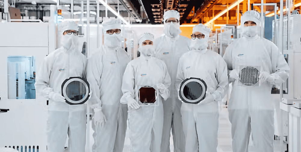
In addition to the latest semiconductor components manufactured on wafers, researchers also presented sensor rings for condition monitoring in mechanical engineering and a laser scanning microscope for the real-time detection of cancer cells in operating theaters. The Fraunhofer Institute has a long-standing cooperation with the most important French research institute CEA-Leti (Commissariat à l’énergie atomique et aux énergies alternatives CEA) – for example in microelectronics on 300-millimeter wafers. The joint projects also have great European relevance within the framework of the EU Chips Act. The initiative aims to strengthen Europe’s competitiveness in semiconductor applications and prevent bottlenecks in this area. As a contribution to the EU Chips Act, a European consortium led by the Research Fab Microelectronics Germany (FMD) is planning to establish the most comprehensive and advanced pilot line for “Advanced Heterogeneous System Integration and Advanced Packaging” in the coming years. CEA-Leti is an important partner in this project.
In order to further promote and expand the cooperation between the Fraunhofer and CEA institutes, François Jacq, President of the CEA, and Prof. Axel Müller-Groeling, Fraunhofer Executive Board Member for Research Infrastructures and Digitization, signed a Memorandum of Understanding (MoU) during the visit. The aim is to initiate a closer exchange and joint initiatives in the strategic areas of microelectronics, quantum technologies, solar and hydrogen technologies, circular economy of CO2 and critical raw materials as well as state-of-the-art battery technology.
Prof. Müller-Groeling explained: “Cooperation across national borders is shaping our future. The close links with partners such as the CEA on the one hand and industry on the other enable us to jointly put key technologies into practice and strengthen our recognition as a driver of innovation in European industry. With applied research in particular, we are thus making a significant contribution to the technological sovereignty and competitiveness of Europe as a business location.”
François Jacq emphasized: “I am delighted with the signing of this agreement between the CEA and Fraunhofer, two leading research partners in Europe, at a time when it is necessary to move forward together to meet the challenges of a more sovereign, greener and more inclusive Europe. This agreement will allow us to develop and expand cooperation in the strategic areas of microelectronics, quantum technologies, solar technology, hydrogen, circular economy and critical raw materials.”
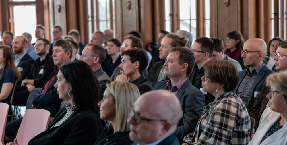
The MoU signing was followed by a round table discussion with both presidents and invited guests on the topic of artificial intelligence, during which Prof. Katharina Hölzle, Director of the Fraunhofer Institute for Industrial Engineering IAO, took part on behalf of the Fraunhofer-Gesellschaft.
About Fraunhofer IPMS
The Fraunhofer Institute for Photonic Microsystems IPMS researches and develops intelligent industrial solutions in the fields of manufacturing, medical technology, healthcare and mobility for microchip producers, suppliers, device manufacturers and R&D partners. Research focuses on miniaturized sensors and actuators, integrated circuits, wireless and wired data communication and customized MEMS systems. Research and development on 200 and 300 millimeter wafers takes place in two ultra-modern clean rooms. The institute’s services range from design and process development to pilot series production. Fraunhofer IPMS is uniquely positioned in Germany in the field of applied research on the modern 300-millimeter wafer industry standard in the front end of CMOS production.
About FMD
The Research Fab Microelectronics Germany (FMD), a cooperation between the Fraunhofer Group for Microelectronics, the Ferdinand-Braun-Institut, Leibniz-Institut für Höchstfrequenztechnik (FBH) and the Leibniz-Institut für innovative Mikroelektronik (IHP), is the central point of contact for all issues relating to microelectronics and nanoelectronics in Germany and Europe. As a one-stop store, FMD has been combining scientifically excellent technologies and system solutions from its 13 cooperating institutes from the Fraunhofer-Gesellschaft and Leibniz Association into a customer-specific overall offering since 2017. Under the virtual umbrella of FMD, the largest association of its kind in Europe has thus been created, with more than 4900 employees and a unique diversity of expertise and infrastructure.
– – – – – –
Further links
👉 www.ipms.fraunhofer.de
Photo: Fraunhofer IPMS
