Organic semiconductors are key components in organic electronics and photovoltaics. They are used to manufacture flexible electronic devices and printed solar cells. Typical for this class of materials are low-temperature processes and large-area deposition and structuring using various coating and printing processes. The active semiconductor materials significantly determine the performance of the entire system. Therefore, an easy-to-use and reliable electronic characterization of conductivity, charge carrier mobility, contact resistance and on/off current ratio of these semiconductors is an essential requirement for material and process developers.
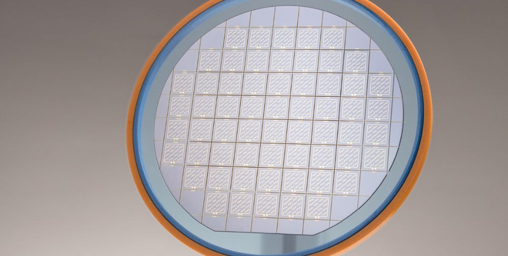
Fraunhofer IPMS develops and manufactures silicon substrates with single transistor structures in bottom-gate architecture, which are used to produce organic field-effect transistors (OFETs) or for the characterization of electrical material parameters of conductive materials, e.g. for organic photovoltaics.
Project manager Thomas Stoppe explains: “Our substrates are already established in the field of R&E at international research institutions. We now want to focus more on customer-specific solutions and are continuously developing the technology further in order to be able to increasingly meet the requirements of industrial partners. There is a rapidly growing market, particularly in the field of organic electronics, and our substrates enable targeted, simple and reproducible measurement of the electrical properties of semiconductors and conductive materials.”
The possibilities for material characterization were demonstrated with recent results, such as the investigation of a commercial graphene emulsion. These results will be presented at the iCampus-Cottbus Conference iCCC2024 in Cottbus in May 2024 and subsequently published in the Journal of Sensors and Sensor Systems.
The developed chips will be presented at the “analytica” trade fair in Munich from April 9 to 12. Interested users will have the opportunity to talk to experts at the Fraunhofer IPMS stand A3.407. Appointments can be made in advance via the Fraunhofer IPMS website.
Advantages of the Fraunhofer IPMS substrates
Access to the existing microsystem technology of Fraunhofer IPMS offers decisive advantages, including the highly precise and reproducible production of the chips and the flexible adaptation of the technology to the individual needs of the target application. Different material combinations and customer-specific adaptations of electrode structures or dielectric thicknesses are possible. This allows high-quality gate oxides with layer thicknesses of 28 nm to 320 nm, which results in extremely low gate leakage currents down to the lower pA range and thus leads to highly accurate measurements. Various orientations of the transistor structures are provided in order to investigate the influences of the deposition process.
Fabrication takes place in a clean room on silicon wafers with thermal silicon dioxide (SiO2). A patented indium tin oxide (ITO) layer acts as a gold adhesion layer, which improves reliability, precision and reproducibility and enables the use of these substrates for comprehensive quality assurance in small and large chemical companies.
About Fraunhofer IPMS
The Fraunhofer Institute for Photonic Microsystems IPMS stands for applied research and development in the fields of intelligent industrial solutions, medical technology and mobility. Research focuses on miniaturized sensors and actuators, integrated circuits, wireless and wired data communication as well as customer-specific MEMS systems. Research and development takes place on 200 and 300 mm wafers in the two clean rooms. The services offered range from consulting and process development to pilot series production.
– – – – – –
Further links
👉 www.ipms.fraunhofer.de
Photo: Fraunhofer IPMS