The three-year project, coordinated by CEA-Leti, brings together 58 partners from across the European semiconductor value chain, from large industrial companies and SMEs to research institutes, universities and industry associations. The project will drive innovative solutions in the areas of emissions control, green materials and alternatives to PFAS-based materials, waste minimization and raw material reuse, in line with the European Green Deal and the EU Chips Act.
“GENESIS addresses the complex challenges of building a truly sustainable semiconductor ecosystem,” says Laurent Pain, Head of the Sustainable Electronics Program at CEA-Leti. “The project structure reflects both the urgency and the opportunities of the green transition in Europe and is supported by the complementary expertise and close collaboration of all partners.”
Fraunhofer IPMS in the project: minimizing chemical waste and reducing emissions
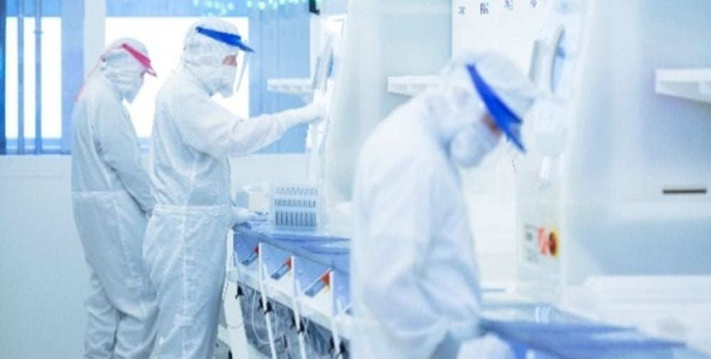
Fraunhofer IPMS is leading one of the central work packages in the project on minimizing chemical waste and reducing emissions. The institute is also investigating the substitution of harmful materials and substances used in semiconductor production. The focus here is on PFAS chemicals (perfluorinated and polyfluorinated alkyl substances) and climate-damaging gases within the BOSCH process. The corresponding work area investigates and improves recycling techniques and exhaust gas cleaning systems, including the development of newer and more efficient cleaning systems.
“The careful use of resources is at the heart of our research within the GENESIS project,” says Dr. Erik Schumann, scientific director of the project at Fraunhofer IPMS. “We are concentrating on replacing and reducing the emission of climate-damaging gases such as SF6 or NF3. These gases are 10,000 times more harmful than CO2, but are needed in the semiconductor industry. We are also working to reduce the waste produced during chemical-mechanical polishing,” he adds.
45 sustainable goals for Europe’s semiconductor chip agenda
According to Laurent Pain, head of the project, around 45 sustainability-oriented innovations covering the entire life cycle of semiconductors are expected, based on four strategic pillars that form the technological foundation of the GENESIS vision for a green European semiconductor industry:
- Pillar 1 – Monitoring and sensing: Real-time emissions tracking, traceability and process feedback systems,
- Pillar 2 – New materials: PFAS-free chemicals and low GWP alternatives for advanced semiconductor processes,
- Pillar 3 – Waste minimization: innovations in recycling (solvents, gases, slurries), reuse and sustainable substitutes and
- Pillar 4 – Critical raw material reduction: strategies to reduce dependence on CRM and strengthen resource security.
In addition to these pillars, the objectives of the project form an overall framework that provides for the use of sensor-integrated reduction systems to reduce PFAS and greenhouse gas emissions. It also aims to position Europe as a pioneer in green semiconductor innovation by aligning supply chain operations with environmental regulations.
A green fit for the EU Chips Act
“GENESIS is a crucial step in aligning Europe’s semiconductor ambitions with its climate change commitments,” said Anton Chichkov, program manager at Chips Joint Undertaking (Chips JU), a public-private partnership established to strengthen the European semiconductor industry by fostering collaboration between the EU, member states and the private sector.
“As chips become the backbone of everything from AI to energy systems, their environmental footprint is growing rapidly,” he adds. “GENESIS is a response to this urgent challenge by pioneering the development of sustainable alternatives in the areas of materials, waste reduction and resource efficiency. With this initiative, Europe is not only investing in greener technologies, but also positioning itself as a world leader in environmentally friendly semiconductor manufacturing.”
The GENESIS project, funded with almost 55 million euros, is co-funded by the European Commission, the participating EU Member States and the Swiss State Secretariat for Education, Research and Innovation as part of the Chips Joint Undertaking.
– – – – – –
Further links
👉 www.ipms.fraunhofer.de
Photo: Fraunhofer IPMS