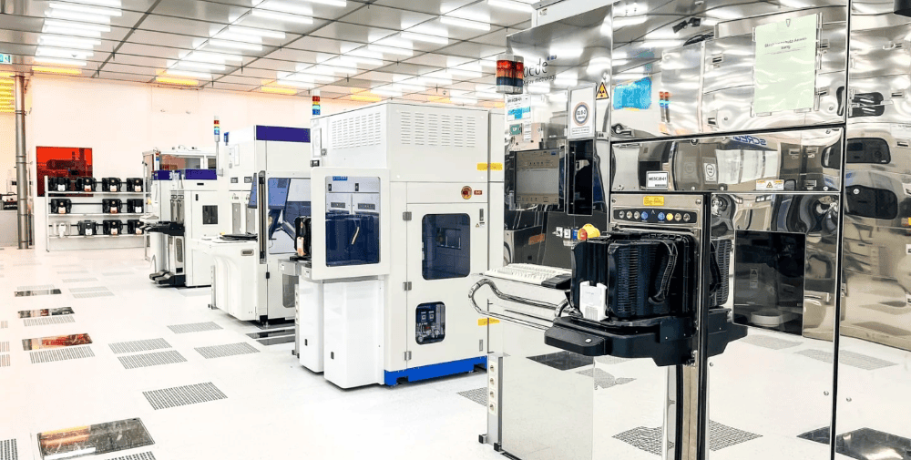
At the heart of CEAM is the Fraunhofer IPMS 300-mm research cleanroom in northern Dresden, which is equipped identically to the cleanrooms of large semiconductor factories. Wafers can therefore be exchanged between industrial production cleanrooms and the CEAM’s cleanroom and analyzed under conditions that closely resemble real-world scenarios. This gives companies the opportunity to test measurement methods using their own wafers on the available systems and evaluate them for their processes—without having to install the systems in their own production facilities beforehand.
Highly specialized measurement systems from PVA TePla form the technical backbone of the CEAM and support critical steps in semiconductor production and quality assurance. The VEreveal fusion hyperspectral system is already in operation for precise material characterization; LuXpector THEA, which combines ellipsometry and reflectometry for non-destructive analysis of thin films, is set to be added soon. Looking ahead, the CEAM is set to be expanded with additional systems from PVA TePla’s portfolio: In addition to a system for measuring stress in wafers (SIRD), a system for acoustic microscopy is also planned to complement the optical focus.
“Our goal is to set new standards in non-destructive material analysis,” says Martin Landgraf, project manager at Fraunhofer IPMS. “The focus is on industrial benefits: High-precision material analyses are intended to help make manufacturing processes in the semiconductor industry more efficient.”
“With the CEAM, we are bringing our measurement technology into an environment that mirrors a modern semiconductor fab,” says Dr. Philipp Wollmann, Managing Director of PVA Vision. “Located in the heart of Europe’s most important microelectronics cluster, customers can test our systems there with their own wafers under real manufacturing conditions. This can significantly shorten evaluation and qualification processes. At the same time, we benefit from direct feedback from the experts at Fraunhofer IPMS, which is immediately incorporated into the further development of our products.”
Through the CEAM, Fraunhofer IPMS and PVA TePla are strengthening Dresden’s position as a hub for semiconductor technologies in Europe. The partnership combines industry-oriented cutting-edge research with applied measurement technology, thereby providing a significant boost to “Silicon Saxony.” Further multiplier effects will result from the integration of CEAM into the European APECS pilot line (APECS—Advanced Packaging and Heterogeneous Integration for Electronic Components and Systems), which, as part of the EU Chips Act, makes state-of-the-art production technologies available for new semiconductor products.
– – – – –
Related Links
👉 www.ipms.fraunhofer.de
👉 www.pvatepla.com
Photo: Fraunhofer IPMS