The Research Fab Microelectronics Germany (FMD) is working intensively in the field of heterointegration and is driving forward chiplet innovations in the APECS pilot line launched at the end of 2024 at European level. A significant portion of the total 730 million euros in APECS funding will go towards technological enablement for chiplets.
These open up ground-breaking opportunities for the automotive industry and high-performance computing in particular, but also for other sectors such as industrial electronics and medical technology. They enable advances in advanced packaging, the integration of powerful subsystems (e.g. high-performance computer modules, sensor/edge modules, control units) and a more flexible supply chain through the use of semiconductor components from different manufacturers.
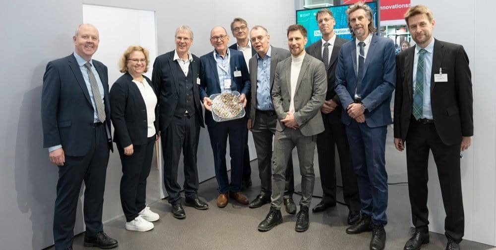
In order to specifically promote the industrial application of chiplets in Germany and Europe, FMD is now setting up the “Chiplet Application Hub”. This forms the application framework for the APECS pilot line and will ensure that companies benefit from the latest chiplet developments and that European strengths in the semiconductor sector can be further expanded. FMD and industry partners from all areas of the semiconductor ecosystem are pooling their expertise in the hub to jointly create new chiplet solutions for applications in the automotive and automation environment. Specific development roadmaps and pilot projects will be created that are specifically tailored to the requirements of the industry. The industrial partners will make significant contributions of their own to drive chiplet innovations forward together with FMD. In combination with the technological possibilities of the APECS pilot line, new production technologies, design methods and standards can be developed and prototypes tested. The “Chiplet Application Hub” acts as a driver of pre-competitive industrial research and raises it to a new level. This enables innovations to reach industrial application more quickly.
Chiplet technology as a catalyst for value creation, technology transfer and competitiveness
The importance of chiplet technology lies in its modularity and scalability. It makes it possible to combine different semiconductor technologies in a targeted manner and tailor them to specific applications. As a result, new system architectures with improved energy efficiency, performance and reusability of individual, very expensive design components can be realized.
Prof. Holger Hanselka, President of the Fraunhofer-Gesellschaft: “The establishment of the ‘Chiplet Application Hub’ marks a further milestone for microelectronics research in Germany, from which Europe will also benefit enormously as a location thanks to an independent, high-performance semiconductor industry. Close cooperation between science and industry will enable us to make targeted and optimal use of the innovative power of chiplet technology.” This is an excellent example of how strong partnerships between leading European research institutions and companies are the key to technological resilience and the basis for groundbreaking innovations, emphasizes Hanselka. “In addition, the establishment of imec in Baden-Württemberg clearly demonstrates how strategic cooperation across national borders can sustainably strengthen Europe’s competitiveness.”
Prof. Albert Heuberger, Chairman of the FMD Steering Committee and Spokesman of the Fraunhofer Group for Microelectronics and Founding Director of the “Chiplet Application Hub”, adds: “The ‘Chiplet Application Hub’ is an important building block for the implementation of the EU Chips Act in Germany and will be closely interlinked with the competence centers that are gradually being established in this context in all European countries. imec’s decision to locate in Heilbronn underlines the close integration of the various players in the European chip ecosystem and shows how the EU Chips Act brings together research institutes, companies and competence centers to jointly ensure Europe’s technological competitiveness.”
Voices from the industry: Advantages of a strategic partnership with the Chiplet Application Hub
The Chiplet Application Hub is based on close cooperation with strong industry partners to develop practical and industry-oriented solutions. By combining design, system integration and test procedures, the hub aims to establish itself as a long-term platform for the application of chiplet technologies in Germany and Europe. Especially in the field of high-performance computing and artificial intelligence, modular semiconductor architectures offer great potential.
“Chiplet technology is a crucial building block for the future of the semiconductor industry,” says Dr. Heike Riel, IBM Fellow, who heads the science of quantum and information technology at IBM, and adds: “Through the modular integration of semiconductor components, we can create innovative computing solutions that are not only more powerful, but also more energy-efficient. The ‘Chiplet Application Hub’ provides an ideal platform to further develop this technology and drive its industrial implementation.”
Chiplet technology also opens up new possibilities for powerful and adaptable electronic systems in the automotive sector.
Jürgen Heckelmann, Head of Strategic Semiconductor Management Procurement at Audi AG, welcomes the establishment of the hub and says: “Chiplets offer enormous advantages for the automotive sector. The transformation towards centralized control units requires flexible and scalable solutions. Especially in automated driving and infotainment, chiplets will enable more targeted adaptation to different vehicle classes and functionalities and also offer more energy-efficient, low-power solutions. Another important advantage lies in the modularization of sensor and actuator systems, allowing them to be integrated more flexibly into different systems. The hub will be an essential partner for the further development of future electronics architectures.”
Andreas Aal, Volkswagen Commercial Vehicles, Senior Member IEEE, CRP, Chair SEMI GAAC adds: “In the long term, chiplets will enable us to create customized hardware platforms specifically for the software-based Mobility & Transport-as-a-Service business model that offer the necessary flexibility, adaptivity and cost efficiency. The ‘Chiplet Application Hub’ forms a crucial bridge to enable digital innovations from the non-automotive sector for use in vehicles in terms of life cycle management, cyber security and robustness. We need to move away from the classic automotive ecosystem and instead become a robust system-of-systems compatible with the global digital ecosystem.”
And Siemens Digital Industries also believes that the heterogeneous integration of chiplets is the way forward for next-generation electronic products, such as autonomous transportation. Heiko Dudek, 3D IC & Advanced Heterogeneous Packaging EMEA, Siemens Digital Industries, explains: “For this reason, investments are currently being made in the development of design technologies and solutions to better serve this area. We welcome the creation of the Chiplet Application Hub and look forward to collaborating on this endeavor to ensure its success.”
By leveraging industry research and technology transfer, the Chiplet Innovation Hub will accelerate innovation and serve as a catalyst for bringing new chiplet technologies to market. In the coming years, the hub will be further expanded through targeted collaborations, research projects and the establishment of a strong innovation network in order to strengthen Germany’s competitiveness in the long term.
Cooperation with strong partners for a strong chip ecosystem
By establishing the “Chiplet Innovation Hub”, FMD is sending a clear signal for the central role of chiplets in microelectronics research and strengthening its position in the European chip ecosystem. The planned establishment of renowned research centers, such as the Belgian “imec”, underlines the relevance of this technology. Imec is planning to set up a research group for chiplet architectures in high-performance computing for the automotive sector in Heilbronn (Baden-Württemberg). In order to make optimum use of this potential, both partners are joining forces and have signed a Memorandum of Understanding (MoU) to define a joint strategic direction. This reaffirms their commitment to driving chiplet innovations forward and setting new standards for their development and industrial application.
– – – – – –
Further links
👉 www.eas.iis.fraunhofer.de
Photo: Fraunhofer / Markus Jürgens