Piezoelectric layers play a central role in medical technology, microelectronics and sensor technology, particularly in the manufacture of ultrasound microscopes. These microscopes make it possible to examine ever smaller structures, such as semiconductor components or biological cells.
Piezoelectric thin films are highly crystalline layers in which the material is deformed when an electrical voltage is applied, allowing sound pulses to be emitted, for example. Ultrasonic pulses can be emitted by adapting the layer properties and thicknesses and applying this voltage very quickly. For higher frequencies and thus better resolution of the ultrasonic microscopes, increasingly shorter distances between the sound pulses are necessary. The requirements for coating quality and corresponding process quality therefore increase sharply with increasing target frequency.
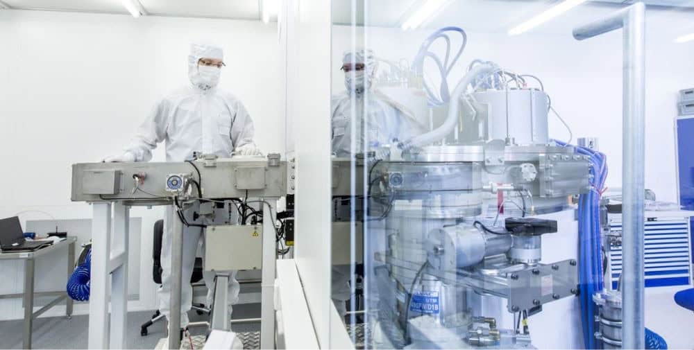
In order to meet these growing requirements, six partners are working on the digitization of coating processes for the production of high-resolution piezoelectric ultrasonic sensors as part of the DigiMatUs joint project funded by the German Federal Ministry of Education and Research (BMBF). In this context, the Fraunhofer Institute for Electron Beam and Plasma Technology FEP in Dresden is developing a digital twin of the coating process for piezoelectric thin films based on aluminum nitride (AlN) and aluminum scandium nitride (AlScN). The coating deposition takes place at the Fraunhofer FEP cluster facilities using pulse magnetron sputtering processes. The various process parameters and influencing factors and their effects on the layer properties are investigated and digitally recorded. The data analysis is based on an ontology for thin-film materials and processes developed jointly with the project partners. An ontology describes a formal system for classifying and structuring knowledge in a specific subject area in order to clearly depict relationships and properties. The resulting digital representation of materials and processes enables precise modelling and optimization of process sequences. This allows process and material properties to be analyzed in detail, which leads to improved performance and reproducibility of the ultrasonic sensors and also makes further development steps more efficient to implement.
“The development of the models poses a particular challenge, as a large number of process parameters and their interactions have to be taken into account. In particular, the comparatively small number of data points combined with a large parameter space places high demands on the development of a robust representation of reality. The Fraunhofer FEP is contributing its many years of expertise in thin-film processing and characterization and thus creating the basis for more efficient and digitally supported production,” explains Dr.-Ing. Stephan Barth, project manager at the Fraunhofer FEP.
The project uses state-of-the-art technologies such as ontologies and artificial intelligence (AI) to analyze and describe the relationships between the process parameters. For example, predictions can be made about how changes in the coating process – such as the adjustment of cathode voltages, substrate temperature or coating pressure – influence the material properties. This enables targeted optimization of the coatings and improves the efficiency of process development.
In the course of the project to date, a first version of the thin-film ontology has been developed together with the project partners, the digital recording and processing of system and process parameters of the systems at Fraunhofer FEP has been expanded, and various material properties of the thin films on the glass bodies of the lenses have been determined as a function of these parameters. Test substrates were coated at the Fraunhofer FEP facilities and handed over to the project partners to enable characterization along the rest of the value chain. The data collected so far forms the basis for the development of the AI models of the project partner Otto von Guericke University Magdeburg. Over the course of the project, the ontology and AI models will be successively developed further in order to better reflect reality. The models developed will be used to further coat test substrates for characterization at the Fraunhofer FEP and at the project partners to improve the models.
In addition to optimizing ultrasonic sensor technology, the project results also open up new possibilities for other applications based on thin-film technologies. The digital mapping of the material and process data by the thin-film ontology and the AI models can be reused and transferred to similar coating processes, which will greatly accelerate the research and development of new materials in the future.
Project information
DigiMatUs – Digitalization of materials research on thin-film materials using the example of high-resolution piezoelectric ultrasonic sensors
Funding body: Federal Ministry of Education and Research
Funding code: 13XP5187D
Project duration: 01.04.2023 – 31.03.2026
Project partner:
- PVA TePla Analytical Systems GmbH
Digitization of coating processes and material research of piezoelectric ultrasonic sensors
- scia Systems GmbH
Definition of the hardware interface to the sensor technology
- Plasus GmbH
Digitalization of process diagnostics for vacuum deposition processes
- Fraunhofer FEP
Digital description of deposition processes for piezoelectric thin films
- Otto-von Guericke University Magdeburg
Ontology development and neurosymbolic predictions for piezoelectric thin film deposition processes
- Technical University Bergakademie Freiberg
Characterization and simulation-driven optimization of thin film systems for ultrasound microscopy
– – – – – –
Further links
👉 www.fep.fraunhofer.de
👉 www.materialdigital.de/project/16
Photo: Fraunhofer FEP, Photo: Anna Schroll
