“In the ‘KoVoPack’ project, we are working with our partners to develop a holistic technology platform with new processes, technologies and systems that can be used to produce fully integrated electronic systems, so-called ‘system-in-package’ (SiP) solutions, efficiently and cost-effectively. In this way, we are creating important foundations for modern communication and experience worlds that will become possible with the two mobile networks 5G and 6G,” says Dirk Wünsch, head of the “Wafer Bonding and Integration Technologies” group and project manager at Fraunhofer ENAS, explaining the objectives of the project.
Together with research partners from industry and science, the Chemnitz-based Fraunhofer Institute is part of the three-year project, which will give the new mobile communications standards a significant development boost. Infineon Technologies Dresden GmbH & Co KG as a semiconductor manufacturer, VON ARDENNE GmbH as an expert in vacuum process technology, the microchip manufacturer SAW components Dresden GmbH and Chemnitz University of Technology are also involved. The project is co-financed by the European Regional Development Fund (ERDF). In addition, this measure is co-financed by tax funds on the basis of the budget approved by the Saxon state parliament.
Focus on increasing miniaturization
“The motivation behind the project idea is that today’s technical devices are becoming ever smaller and flatter, but should be equipped with ever more sophistication and functionalities. The progressive miniaturization of technical products requires a constant reduction in the size of the microelectronic components and systems installed in them. Sophisticated technologies, material concepts and assembly and connection techniques are needed to make them even more compact, smaller and flatter in the future, so that they can be used for optical, radio and radar applications and thus for applications in the 5G and 6G networks,” explains the Fraunhofer scientist.
Requirements for enormous storage capacities
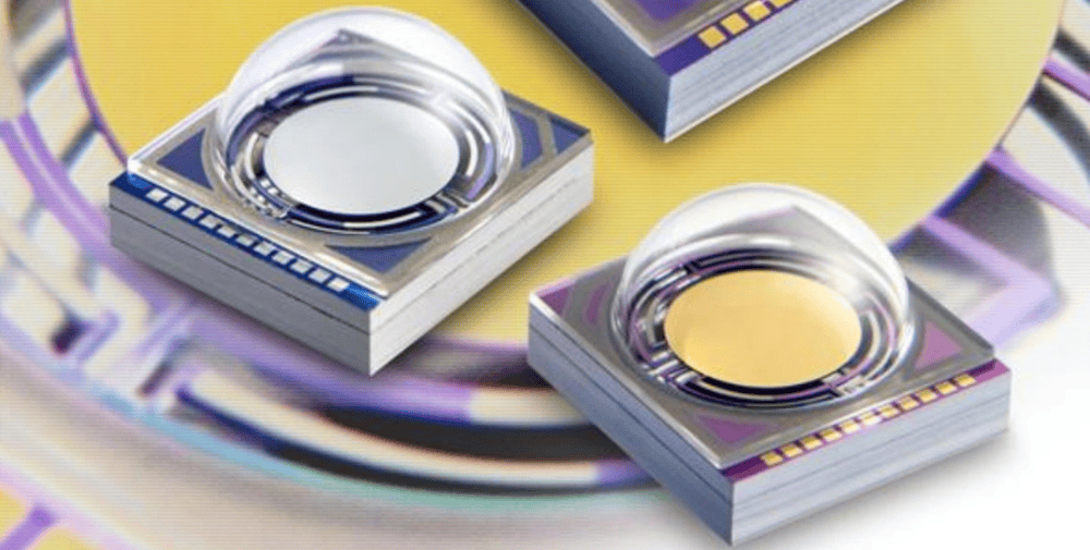
For example, the “KoVoPack” project aims to develop new processes, technologies and systems for phase change materials (PCM) based on the semiconductor material germanium antimony telluride (GeSbTe) in order to produce high-frequency switches and optical components. In the past, phase change materials were mainly used in the area of rewritable blue-ray discs. If they are exposed to thermal influences, they can change their structure between crystalline and amorphous. These structural changes in turn cause a change in their electrical and optical properties. This makes PCMs suitable for the production of photonic and electronic components that are used in display and storage technologies, for example. This could result in next-generation smartphones that are characterized by significant energy efficiency, greater memory requirements, long battery life and increased lifetimes as well as higher-resolution displays. Based on PCMs, RF switches can also be realized that can be used in antennas and antenna tuners. In this way, better signal transmission and quality and therefore optimum mobile phone coverage can be achieved. Finally, PCMs are also “enablers” for integrated photonics and allow the production of modulators, tunable resonators, photonic memories and optical filters that function entirely without moving components. One conceivable future application would be photonic neuromorphic computing, which would make computers for artificial intelligence significantly faster and at the same time more energy-efficient.
As part of the project, Fraunhofer ENAS will develop deposition processes based on physical vapour deposition (PVD) for phase change materials, research methods for their structuring and characterize the realized materials using analytical methods with the aim of being able to integrate them into future component concepts.
Accelerated data transmission and new control concepts
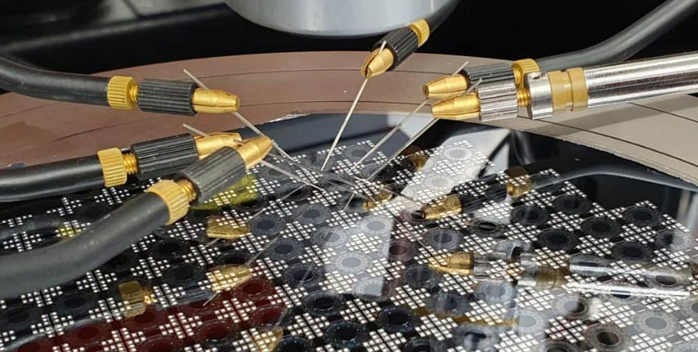
Small and flat electronic modules for 5G and 6G applications require significantly more compact and, above all, hermetically sealed wafer-level packages to protect them from moisture ingress and ensure their continuous performance. With its proven and long-standing expertise in the field of wafer bonding techniques with various substrates, Fraunhofer ENAS will support the achievement of this goal within the framework of “KoVoPack”. The aim is to develop new wafer bonding processes for wafer-level packages based on silicon-based bipolar CMOS (BiCMOS) wafers as well as compact solutions for hermetic encapsulation and electrical contacting.
The assembly and connection technologies developed in the project will contribute to the production of efficient high-frequency modules, for example. As the introduction of 5G and the next development stage, 6G, will give rise to completely new applications in the field of Industry 4.0 and autonomous driving, which require the transmission of significantly larger amounts of data at higher transmission speeds, more powerful radio frequency modules can be used to transmit huge amounts of data in even less time. The emerging assembly and connection technologies are also of interest for radar-based gesture recognition sensors. Highly sensitive sensors allow, for example, the intelligent operation and control of the latest smartphones via the finest movements of their users without any physical contact.
The technologies and processes developed as part of the “KoVoPack” project will overcome an important hurdle in industrial production in order to manufacture new components for 5G and 6G applications. This should pave the way for the introduction and market penetration of the new communication standards.
– – – – – –
Further links
👉 www.enas.fraunhofer.de
Photo: Fraunhofer ENAS