Europe has a dynamic ecosystem of leading companies in traditional industries, small and medium-sized enterprises (SMEs) and start-ups, whose competitive advantage is also based on advanced semiconductor solutions that form the basis for innovation. However, these companies today face the challenge of limited access to advanced technologies due to a lack of resources in Europe. As part of the EU Chips Act, the European Commission is investing considerable resources in strengthening semiconductor technologies and applications in the EU. The aim is to increase Europe’s technological resilience, secure supply and value chains and drive innovation in key sectors such as artificial intelligence, mobility, manufacturing, information and communication technologies, trustworthy and environmentally sustainable electronics as well as neuromorphic and quantum computing.
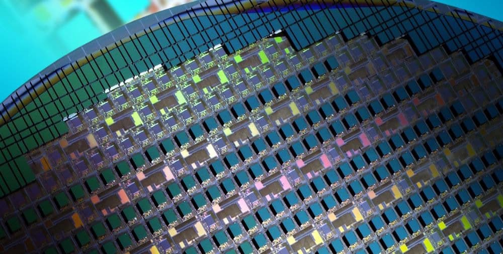
The APECS pilot line focuses on the scalable industrial transfer of newly developed innovations in the field of heterointegration*, in particular the use of new chiplet** technologies, thus building a bridge to application-oriented research. APECS goes beyond traditional system-in-package (SiP) methodologies and aims to deliver robust and trustworthy heterogeneous systems that significantly increase the innovation capability of the European semiconductor industry.
Investing in strategic projects such as APECS under the EU Chips Act is crucial to position Europe as an indispensable partner in the global technology industry. Germany plays a key role in this endeavor – both as a leading research location and as a driving economic force. Thanks to substantial funding from the Federal Ministry of Education and Research (BMBF) and the federal states of Saxony, Berlin, Bavaria, Schleswig-Holstein, Baden-Württemberg, North Rhine-Westphalia, Brandenburg and Saxony-Anhalt, it will be possible to further expand the R&D infrastructure within the APECS pilot line in the coming years. This is an important step towards securing the long-term economic stability of Germany and Europe.
“Fraunhofer plays a central role in the implementation of large-scale projects such as APECS, which strengthen Germany’s innovative strength and technological resilience,” emphasizes Prof. Holger Hanselka, President of the Fraunhofer-Gesellschaft. “Through our practical research and close cooperation with industry, science and political partners, we create the basis not only for developing the latest technologies, but also for bringing them into industrial application. The APECS pilot line is an example of bridging the gap between research and industry and underlines how close cooperation with ministries and other partners can sustainably secure Europe’s position in the global microelectronics market.”
Innovations exactly where European industry needs them most
The APECS pilot line aims to enable new functionalities through System Technology Co-Optimization (STCO) and standardize integration technologies. This will enable companies to develop advanced products even in small quantities at competitive costs. By providing a variety of technologies in a one-stop-shop, APECS will become Europe’s leading hub for advanced packaging and heterointegration, playing a key role in European microelectronics.
As a driving force for collaboration between European research institutions, industry and academia, the APECS pilot line fosters a vibrant innovation ecosystem. As a comprehensive platform, APECS integrates end-to-end design and pilot production capabilities, enabling the advancement of innovations from cutting-edge research to viable, scalable manufacturing processes.
APECS will play a crucial role in Europe’s transition to a climate-neutral and circular economy by driving eco-design and sustainable manufacturing initiatives.
Innovation through strong collaboration on multiple levels
The APECS pilot line builds on the structures created in the Research Fab Microelectronics Germany (FMD). In Germany, a total of twelve institutes from the Fraunhofer Group for Microelectronics and the two Leibniz institutes FBH and IHP are involved in APECS. The work is led by the office in Berlin.
Prof. Albert Heuberger, spokesman for the Fraunhofer Group for Microelectronics and Chairman of the FMD Steering Committee, emphasizes: “The success of the EU Chips Act is based on strong partnerships and diverse expertise. This is exactly what the FMD brings to the table by combining the strengths of decentralized research institutions. APECS also builds on this foundation and can therefore become a long-term accessible pilot line for all European stakeholders across the entire value chain. Together with the other pilot lines under the EU Chips Act, APECS is a crucial component for heterointegration and advanced packaging of an overarching pan-European microelectronics pilot line.”
In a strong European consortium, APECS bundles the technological competencies, infrastructures and know-how of a total of ten partners from eight European countries: Germany (Fraunhofer-Gesellschaft as coordinator, FBH, IHP), Austria (Graz University of Technology), Finland (VTT), Belgium (imec), France (CEA-Leti), Greece (FORTH), Spain (IMB-CNM, CSIC) and Portugal (INL). The APECS pilot line is coordinated by the Fraunhofer-Gesellschaft and implemented by the Research Fab Microelectronics Germany (FMD).
About the Research Fab Microelectronics Germany (FMD)
The FMD, a cooperation between the Fraunhofer Group for Microelectronics and the Leibniz Institutes FBH and IHP, is the central point of contact for all issues relating to microelectronic and nanoelectronic research and development in Germany and Europe. As a one-stop store, FMD has been combining scientifically excellent technologies and system solutions from its 13 cooperating institutes from the Fraunhofer-Gesellschaft and Leibniz Association into a customer-specific overall offering since 2017. Under the virtual umbrella of FMD, the largest association of its kind in Europe has thus been created, with more than 4900 employees and a unique diversity of expertise and infrastructure. www.forschungsfabrik-mikroelektronik.de
*About Heterointegration
Semiconductor research and development is at the heart of current technological (r)evolutions, ranging from artificial intelligence and high-performance computing to modern defense systems, robotics, power electronics, wireless communication, e-health, quantum technologies and more. Such future electronic systems will require more and more functions that cannot be performed by a single chip, even if advanced system-on-chip (SoC) concepts are used. Heterointegration will go beyond current system-in-package (SiP) approaches and is critical for next-generation electronic systems and devices based on future CMOS nodes, SiGe, SiC, III/Vs such as GaAs or GaN, and all different types of microelectromechanical systems (MEMS).
**About chiplets
The idea behind chiplets is to use different types of intellectual property (IP) that can be used for specific functions. IP cores are understood to be a multi-purpose, prefabricated functional block of a chip design in the semiconductor industry. This is usually licensed to other IC designers as the intellectual property of the developer in order to integrate it into another, usually larger, IC design. The various blocks are already tested and can be put together like a puzzle, so that existing IC structures can be used and only parts need to be redesigned. A chiplet is therefore not a fully functional individual chip, but a part of a chip that can be combined with other functional elements. The concepts and initial implementations of chiplets not only promise higher integration densities, but also touch on environmental properties of electronics in terms of resource efficiency, critical raw materials, modularity and reusability of design blocks.
– – – – – –
Further links
👉 www.enas.fraunhofer.de
Photo: Fraunhofer ISIT


