February 9, 2024. The Federal Ministry of Education and Research is promoting a new format for networking and expanding expertise and capacities in chip design in order to strengthen the technological sovereignty of Germany and Europe.
Categories
February 9, 2024. The Federal Ministry of Education and Research is promoting a new format for networking and expanding expertise and capacities in chip design in order to strengthen the technological sovereignty of Germany and Europe.
Categories
Tags
Contact info
Silicon Saxony
Marketing, Kommunikation und Öffentlichkeitsarbeit
Manfred-von-Ardenne-Ring 20 F
Fax: +49 351 8925 889
Contact person:
![]()
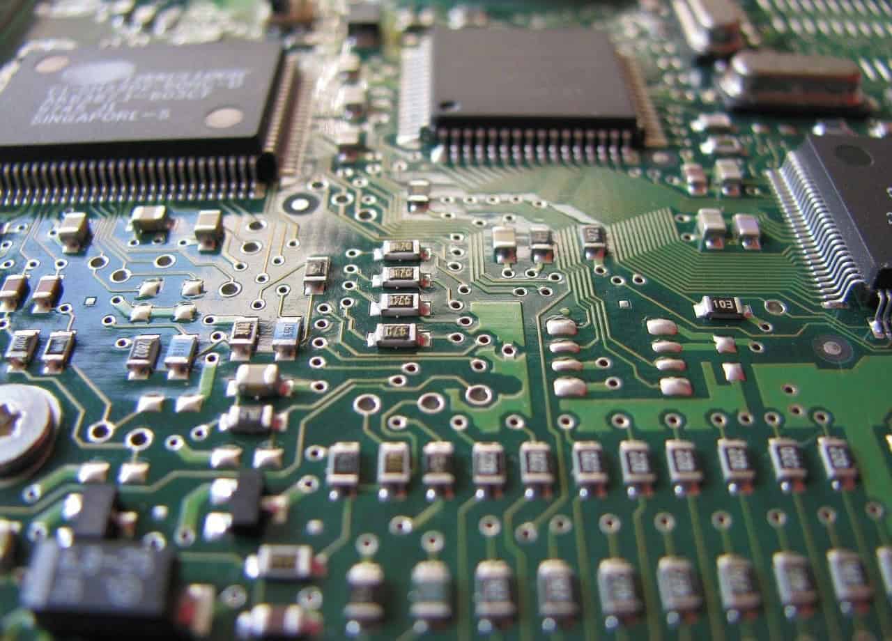
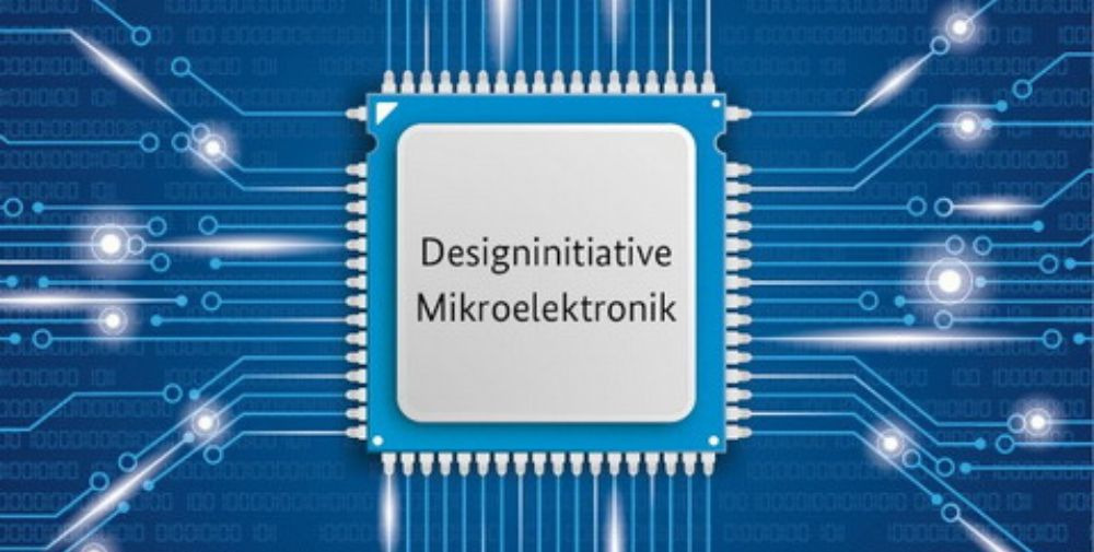
Whether cars, cell phones or washing machines: no electrical device can do without an integrated circuit. Chip design is the essential step in designing microelectronics for future products and applications. With this in mind, the Federal Ministry of Education and Research (BMBF) is funding the new “Chipdesign Germany” network for three years with four million euros as part of the microelectronics design initiative. It is motivated by the conviction that expertise in chip design can strengthen Germany’s innovation and competitiveness and gain technological sovereignty in Europe.
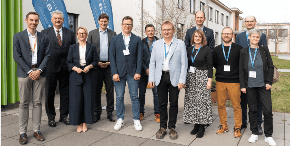
The “Chipdesign Germany” network forms a platform for pre-competitive, open exchange between all players involved in chip design. It is supported by the four cooperation partners edacentrum GmbH, Forschungsfabrik Mikroelektronik Deutschland, Rheinland-Pfälzische Technische Universität Kaiserslautern-Landau and Leibniz Universität Hannover.
The task of the network is to give chip design a voice in order to make its importance for the economy and society visible. “Chipdesign Germany” serves as a central point of contact for this topic in Germany and develops and networks measures for the training and further education of young professionals, technology monitoring, support for start-ups and small and medium-sized enterprises in microelectronics and science communication in order to raise awareness of the topic in society. The network advises the BMBF on all questions of chip design, Germany’s positioning in microelectronics and develops recommendations for action for accompanying program research.
The edacentrum is an independent authority for electronics, design and applications in business and science. It shapes research & development for a consistent design methodology along the entire value chain. In this role, the edacentrum is a recognized innovation accelerator for the microelectronics industry and its user industries.
The edacentrum initiates, coordinates and supports industry-led, publicly funded R&E projects in the field of EDA, both in the classic sense of “electronic design automation” and in the sense of “electronics, design and applications” and offers a comprehensive range of services.
The Research Fab Microelectronics Germany (FMD) is a globally leading and cross-location R&D association for micro- and nanoelectronics and bundles the expertise and technological infrastructure of its 13 cooperating institutes from the Fraunhofer-Gesellschaft and Leibniz Association throughout Germany. As a one-stop store, it offers scientifically excellent, application-oriented technologies and system solutions for future-oriented microelectronics. It thus makes a decisive contribution to the technological sovereignty of Germany and Europe. From 2017 to 2021, the Federal Ministry of Education and Research supported the modernization of the research infrastructure of all 13 participating institutes. You can find more information at www.forschungsfabrik-mikroelektronik.de. You can also visit our virtual 3D showroom at https://fmd-insight.de/showroom.
Since January 1, 2023, the Technical University of Kaiserslautern and the University of Landau together form the Rhineland-Palatinate University of Technology Kaiserslautern-Landau. With over 20,000 students and more than 300 professors, RPTU is the second largest academic institution in the state. As a place of top international research and an academic talent factory for business and science, RPTU offers excellent study and research conditions as well as a cosmopolitan environment. RPTU is also an innovation and transfer partner for politics, business and society.
As one of the nine leading technical universities in Germany, Leibniz Universität Hannover believes it has a responsibility to contribute to sustainable, peaceful and responsible solutions to key future challenges. The expertise for this arises from the broad spectrum of subjects, which ranges from engineering and natural sciences, architecture and environmental planning, law and economics to research-intensive social sciences and humanities.
Prof. Dr. Norbert Wehn: norbert.wehn@rptu.de
Prof. Dr. Holger Blume: holger.blume@ims.uni-hannover.de
The edacentrum is the network for electronics, design and applications in business and science. As an independent body, the edacentrum shapes research & development for a consistent design methodology along the entire value chain. In this role, the edacentrum is a recognized innovation accelerator for the microelectronics industry and its user industries.
The edacentrum initiates, coordinates and supports industry-led, publicly funded R&D projects in the field of EDA, both in the classic sense of “electronic design automation” and in the sense of “electronics, design and applications”, and offers a comprehensive range of services such as project management for these R&D projects. Furthermore, it organizes the bundling of existing EDA expertise at German research institutions within the framework of EDA cluster research projects and offers innovative technical solutions for exchange and cross-company cooperation.
The edacentrum bundles the interests of industry and science with regard to new challenges in the field of designing microelectronic components and systems and their applications. To this end, it coordinates industry-specific working groups, organizes its own specialist conferences and operates platforms for target group-specific services and public relations work.
– – – – – –
👉 www.chipdesign-germany.de
👉 www.elektronikforschung.de/projekte/chipdesign-germany
👉 www.edacentrum.de
Photo: Chipdesign Germany
You need to load content from reCAPTCHA to submit the form. Please note that doing so will share data with third-party providers.
More InformationYou are currently viewing a placeholder content from Turnstile. To access the actual content, click the button below. Please note that doing so will share data with third-party providers.
More InformationYou are currently viewing a placeholder content from Facebook. To access the actual content, click the button below. Please note that doing so will share data with third-party providers.
More InformationYou are currently viewing a placeholder content from Google Maps. To access the actual content, click the button below. Please note that doing so will share data with third-party providers.
More InformationYou are currently viewing a placeholder content from OpenStreetMap. To access the actual content, click the button below. Please note that doing so will share data with third-party providers.
More InformationYou are currently viewing a placeholder content from Instagram. To access the actual content, click the button below. Please note that doing so will share data with third-party providers.
More InformationYou are currently viewing a placeholder content from X. To access the actual content, click the button below. Please note that doing so will share data with third-party providers.
More Information