The funding is part of Vinnova’s initiative to support deep-tech companies and recognizes the potential of AlixLabs’ APS™ technology to enable cost-effective scaling at the Ångström level for the semiconductor industry.
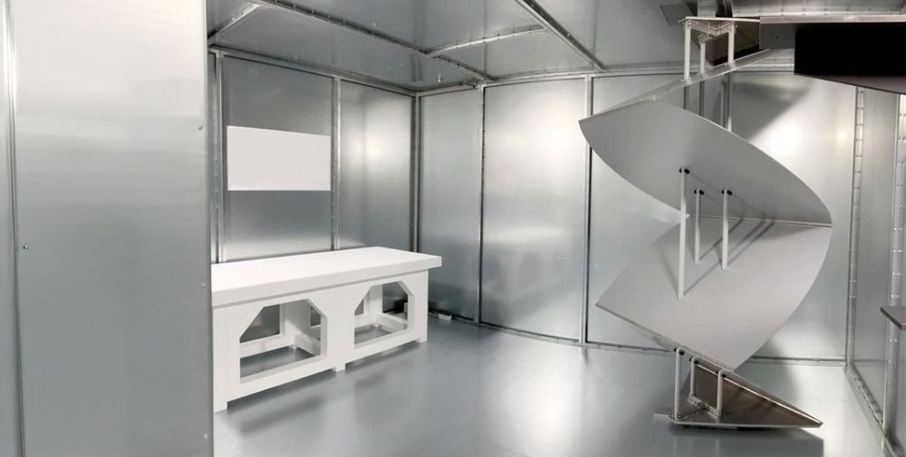
“We are always pleased to receive recognition and government support for our efforts to grow our business and commercialize our technology,” said Amin Karimi, COO and R&D Manager at AlixLabs. “The support comes at a crucial time as we install our first 300-millimeter tool in our cleanroom and increasingly collaborate with potential customers in the semiconductor industry. At the center of our efforts is our APS™ technology, which we believe is the most sustainable and affordable path for semiconductor manufacturing at 3 and 2 nanometers and beyond.”
AlixLabs’ offering includes Atomic Layer Etch Pitch Splitting (APS™) technology, which already enables etching of feature sizes comparable to today’s 3-nanometer class chips using the company’s proprietary equipment. With other proprietary atomic layer etching (ALE) processes, AlixLabs can also contribute to RF and power IC gallium nitride (GaN) and silicon carbide (SiC) workflows, with pattern transfer, precision etching and surface roughness reduction for wafers.
“The semiconductor industry is facing a major challenge in terms of sustainability and rising costs in the production of the latest generation semiconductors. We propose etching instead of costly EUV lithography, and our demonstrations show that we can help produce sub-3 nanometer chips at 35-50 percent lower cost per wafer pass than using EUV,” said Jonas Sundqvist, CEO of AlixLabs. “While we are targeting the leading logic and memory manufacturers with APS™, our technology also enables foundries that have abandoned sub-20 nanometer production to downsize cost-effectively.”
AlixLabs will use the Vinnova grant to accelerate the commercialization of its APS™ technology by intensifying customer engagement and conducting demonstration projects. These demos will be conducted both at AlixLabs facilities and on customer platforms to demonstrate the practical benefits of APS™. This approach is intended to increase the technology readiness level (TRL) of our solutions, pave the way for broader industry adoption, and reinforce AlixLabs’ commitment to providing innovative, cost-effective scaling solutions for semiconductor manufacturing.
– – – – –
Further links
👉 www.alixlabs.com
Photo: AlixLabs
