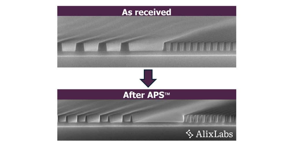
The APS™ technology was tested on 300-millimeter wafers from United Microelectronics Corporation (UMC) and successfully halved the pitch compared to current industry benchmarks. This significant advance was achieved entirely without the use of expensive and energy-intensive extreme ultraviolet (EUV) lithography.
Instead, APS™ utilizes advanced etching techniques that significantly improve sustainability and dramatically reduce power consumption without compromising throughput. Previous demonstrations of the APS™ process, validated by the Intel Test Vehicle Program[1], confirmed its potential by achieving metal gaps as small as 25 nanometers.
“Today we provide further proof that the APS™ process can be game-changing for leading foundries. Thanks to UMC, we were able to verify our process on production wafers that are shipped in quantities of millions of wafers per year,” said Dr. Robin Athle, lead researcher at AlixLabs. “Our mission is to develop equipment that enables companies that do not have access to EUV tools to scale down their production to 5 nanometers and below. By eliminating the reliance on EUV lithography, we offer the industry a path to more sustainable and economically feasible high-density chip production.”
– – – – –
Further links
👉 www.alixlabs.com
👉 www.alixlabs.com/2025/02/07/alixlabs-to-showcase-latest-aps-findings-at-spie-advanced-lithography-patterning/
Photo: AlixLabs