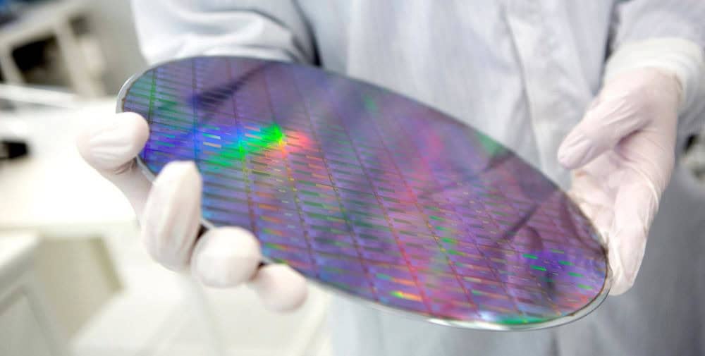
AlixLabs APS™ is designed to reduce the cost of manufacturing sub-7 nanometer products where feature sizes of less than 20 nanometers are required. With APS™, estimated cost savings of up to 40 percent per mask level can be achieved instead of relying on EUV lithography and complex self-aligned multi-patterning processes.
“While our 300-millimeter tool is being put through its paces in our lab, we look forward to demonstrating it to Japanese customers. Japan is investing heavily in revitalizing its semiconductor industry and wants to become a leading player in this business again. With APS™, we can help achieve this at a lower cost both upfront and during mass production, while reducing the carbon footprint of production,” says Amin Karimi, COO and R&D Manager at AlixLabs. “At the show, I am personally looking forward to meeting existing and potential customers and being part of the Japanese semiconductor boom. We have a lot of interest from Japanese customers, and this is the right place for us.”
APS™ and the associated Made in Sweden tools can already produce 20-nanometer half-tone lines and critical dimensions below 15 nanometers on silicon and 3 nanometers on gallium phosphide. There are also numerous applications for power electronics, including precision etching and surface cleaning, each enabling better electrical performance than today’s standard processes.
AlixLabs aims to supply leading semiconductor manufacturers in both the logic and memory segments. At SEMICON Japan, the company will be represented by COO and R&D Manager Amin Karimi in the EU pavilion.
– – – – – –
Further links
👉 www.alixlabs.com
Photo: AlixLabs


