Innovative, small, fast and precise. And a touch of energy efficiency to boot. These are the desired ingredients for many advanced technologies and miniaturized components. Fraunhofer IPMS also offers smaller companies access to its research portfolio, state-of-the-art technologies and equipment as well as the 200 mm and 300 mm cleanrooms so that rapid technological progress can continue.
MEMS technologies and components on 200 mm wafers
Fraunhofer IPMS is responsible for the technological development and support of MEMS technologies along the entire value chain: from individual processes and technology modules to complete technologies, as well as process engineering support for the systems in the cleanroom. i. Following successful development, the institute offers pilot production and technology transfer support. Fraunhofer IPMS thus covers technological readiness levels (TRL) from three to eight. Start-ups, SMEs and companies without their own fabs in particular can thus benefit from low investment costs.
In the field of sensor and actuator technology, for example, Fraunhofer IPMS develops capacitive ultrasonic sensors. These are offered as a platform that can be quickly customized. This also offers SMEs cost-effective access to high technology.
Another important aspect for customers: A simple and cost-effective way to test the latest developments in their application. Fraunhofer IPMS offers evaluation kits for this purpose. With these ready-to-use set-ups, customers can immediately incorporate the microscanner technology into their product development, for example, as the appropriate control electronics to meet the specifications are already included in the scope of delivery. Costly in-house developments are no longer necessary.
300 mm semiconductor process and product development for nanoelectronics
With the Center Nanoelectronic Technologies (CNT), Fraunhofer IPMS conducts applied research on 300 mm wafers for chip manufacturers, suppliers, equipment manufacturers and R&E partners.
A wide range of technology developments and support services are offered in the field of ultra-large-scale integration (ULSI). These include individual process developments in the areas of atomic layer deposition, chemical-mechanical polishing, wafer metallization, wafer cleaning, metrology and nanopatterning. The evaluation and optimization of chemicals and consumables for the latest CMOS technologies as well as system qualifications are also possible in the CNT clean room. The focus of R & D activities is in the front-end area with a focus on the integration of functionalities in wiring levels (BEoL module). This primarily includes various non-volatile memories, capacitors and varactors. Together with Fraunhofer IZM-ASSID (focus on heterointegration and wafer level packaging), the Center CEASAX (Center for Advanced CMOS & Heterointegration Saxony) bundles expertise and focuses on research in the fields of neuromorphic computing, cryo and quantum technology and advanced packaging.
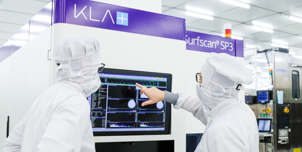
To expand the possibilities, a technology center for semiconductor metrology and process analysis was founded with the company Applied Materials. State-of-the-art eBeam metrology devices from Applied Materials were installed at Fraunhofer IPMS for this purpose. Precise measurement technology is crucial for quality monitoring in the manufacture of microchips in order to validate the physical and electrical properties and ensure the desired yield.
Green ICT – Sustainable information and communication technology
Increasing digitalization presents both opportunities and challenges for environmental protection. Although the intelligent control of devices saves energy, their increasing use also increases energy consumption. Microelectronics therefore needs new approaches to minimize the environmental impact of both production and design. Fraunhofer IPMS is working closely with the Research Fab Microelectronics Germany (FMD) in the Green ICT competence center to actively promote the reduction of resource consumption. This includes energy-efficient sensor edge cloud systems (battery-free sensors as well as neuromorphic AI accelerators) and communication networks (Li-Fi and Ethernet TSN) as well as resource-optimized electronics production on both 200 mm and 300 mm wafers. The latter includes the optimization of material consumption and the replacement of critical materials in the area of wet processes and lithography as well as the optimization of energy consumption and emissions.
Latest research results at “Semicon Europa”
From November 16 to 19, Fraunhofer IPMS will be presenting its latest research results and technologies at the “Semicon Europa” trade fair in Munich. Visitors will have the opportunity to get in touch with the researchers at the Silicon Saxony joint stand #B1-221/33a. Appointments can be made in advance via the Fraunhofer IPMS website. Three other FMD members – Fraunhofer ENAS, Fraunhofer IZM-ASSID and the Leibniz Institute for Innovative Microelectronics (IHP) – will also be represented as part of the Research Fab Microelectronics Germany (FMD).
Further links
👉 www.ipms.fraunhofer.de