Complex and more of a value network than a value chain. The production of microchips is demanding and characterized by numerous dependencies. Our overview shows the interdependencies as well as the work steps and selected top players.
Categories
Complex and more of a value network than a value chain. The production of microchips is demanding and characterized by numerous dependencies. Our overview shows the interdependencies as well as the work steps and selected top players.

Categories
Tags
Contact info
Silicon Saxony
Marketing, Kommunikation und Öffentlichkeitsarbeit
Manfred-von-Ardenne-Ring 20 F
Fax: +49 351 8925 889
Contact person:
In our graphic, we provide an overview of value creation in microelectronics, which is more of a “network” than a “chain” due to the numerous dependencies and individual players involved at various points in the value chain. We have defined a total of eleven important areas. But what exactly do they stand for? We explain this below.
Definition: Design comprises the layout of the electronic circuits (circuits) that are later realized in production in over hundreds of process steps and with a wide variety of materials on the wafers. The layout and design depend on the future task and functionality of the chips. However, this category includes not only the chip level but also the wafer level (e.g. optimum utilization of the surface area and enabling subsequent testing and quality assurance measures) and can even be extended to system level. We also include the tools (software) for EDA and simulation (across the board). In (chip) design, engineers and designers create electronic circuits for computer chips. This step determines how the chip works and what tasks it fulfills.
What this includes: IP, Tools (Software) for IC-Design, Fabless and Design Houses
Known players in the field: arm, Cadence, Synopsis, Nvidia, Racyics
_ _ _ _ _ _
Definition: Wafer manufacturing involves the production of the round substrate disks (wafers) that serve as the basis for the manufacture of computer chips. In the most common cases, the material is still silicon, produced as a single crystal up to 300 mm in diameter (which is cut into 1 mm slices and ground and polished). However, more exotic semi-conductive materials such as silicon carbide (SiC), gallium arsenide (GaAs) or silicon germanium (SiGe), among others, have also been used for a wide variety of applications.
What this includes: Manufacturers of substrate material for microelectronics, Si wafers and other semiconductor substrates (GaAs, SiC, SiGe, etc.)
Known players in the field: Shin-etsu, GlobalWafers, Siltronic, SUMCO
_ _ _ _ _ _
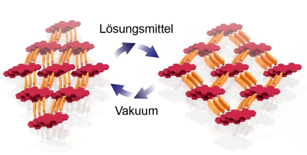
Definition: To transfer the circuit designs (see Design) to the substrates using various manufacturing processes (see Frontend Manufacturing) or to manufacture them, stencils/masks are required. These consist of high-purity glass panes which, unlike the chip substrates (wafers), are square and several millimeters thick. The image of these circuits is imaged onto the substrate/wafer surface in an exposure process – comparable to stencil printing (simplified). The highlight of this process is that the relatively large image of the circuits is reduced to the necessary small size (mm -> nm) using sophisticated optics.
What’s involved: Mask houses, manufacturers of photographic masks (reticles)
Known players in the field: TOPPAN PHOTOMASK, Dai Nippon Printing, Photronics Inc.
_ _ _ _ _
Definition: Front-end manufacturing is the process by which the actual microchips are created on the wafers. This takes place over hundreds of different process steps on complex systems that apply a wide variety of materials in individual layers to the substrate, the wafer, one after the other, process them (polish, structure, partially remove) and thus gradually form the circuits and transistors etc. on the wafer.
What this involves: Contract manufacturers (foundries) and semiconductor fabs that manufacture their own products
Known players in the field: TSMC, Infineon, GlobalFoundries, SAMSUNG Electronics
_ _ _ _ _
Definition: Backend manufacturing includes the separation of the wafers into individual chips (up to several hundred per wafer), the assembly and wiring of the microchips and the production of housings and connections to make the chips manageable, robust and functional for further integration into systems.
What this involves: Chip assembly, separation of Dys (the actual microchip, i.e. the area on the wafer that belongs together), embedding in a housing, packaging (bonding, wiring and encapsulation) and testing
Known players in the field: ASE, AMKOR, JCET, ADVANTEST, SAMSUNG Electronics, Infineon
_ _ _ _ _ _
Definition: Inspection and metrology refer to the testing and measurement during the manufacturing process of chips and wafers in order to identify process errors at an early stage and ensure high quality standards. This includes all measurements in the individual process steps. This includes measuring layer thicknesses, structure sizes and checking the desired material parameters such as conductivity (e.g. charge carrier concentration) in the functional areas/layers of a microchip on the wafers. This also includes process monitoring.
The measurements are carried out both in-line, i.e. in the process, or by sampling and destructive measurements (e.g. electron microscopy and chemical analyses) in order to check in the nm range whether the desired electronic structures have been successfully realized. This also serves to identify the causes of errors and to draw conclusions about optimization potential.
What this includes: Inspection of the chip surfaces, measurement of the size and position of the processed structures as well as localization and identification of defects/errors.
Known players in the field: Applied Materials Inc., Nikon Metrology NV, KLA Corporation, Hitachi
_ _ _ _ _ _
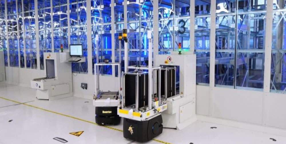
Definition: These are all systems and machines that are required in the individual production steps in the front and back end. Roughly speaking, these are systems for logistics in the fab (robots, transport systems), machines for coating and removing material from the wafer surface, changing the material properties (chemical or electrical) through temperature or bombardment with ions and the introduction of the desired structures from the specifications of the (chip) design via photolithographic processes.
What this includes: Machines, for example for exposing wafers (lithography exposure machines), for etching circuits through to transport through production
Known players in the field: ASML, Applied Materials, LAM, TEL
_ _ _ _ _ _
Definition: Advanced Process Control (APC) refers to technologies and strategies used to monitor and optimize production processes in microelectronics in order to increase efficiency and ensure quality. Special attention is paid here to all matters that go beyond the individual process steps and concern logistics and management from process step to process step.
What this includes:Material logistics, optimization of the entire production operation for optimal utilization of machines and systems, taking into account availability, urgency, maintenance intervals, the actual process and production controlling, automation in all production areas
Known players in the field: Kontron AIS, Peer group, Onto innovation
_ _ _ _ _
Definition: This includes the physical production facilities and buildings in which microelectronics manufacturing takes place. Everything that ensures the supply of the processes and systems with the necessary resources: Piping, connections for media, waste and chemical management as well as the climatic and cleanroom-specific facilities are covered here. This also includes personal equipment for personnel.
What this includes: everything that is necessary to enable cleanroom production, from construction and the cleanroom itself to air conditioning and piping, connection technology and basic production infrastructure
Known players in the field: Exyte, Mercury, DAS EE
_ _ _ _ _ _
Definition: Parts and components include all structural, spare and wear parts as well as materials used in the manufacturing processes of microelectronics.
What this includes: Spare parts (e.g. seals), consumables, various subsystems for machines and process control (e.g. pressure and flow meters)
Known players in the field: Inficon, VAT, Festo
_ _ _ _ _ _
Definition: Chemicals are substances used in manufacturing for cleaning, etching, coating and other processes to produce the wafers and chips.
What this includes: gaseous, liquid and solid (raw) chemicals for all process steps in microelectronics production (photoresists, cleaning solutions, etching agents, coating materials, etc.)
Known players in the field: Linde, Air Liquide, cabot
_ _ _ _ _
This content was published as part of NEXT Microelectronics (November 2023).
_ _ _ _ _