They block leakage currents, i.e. unwanted power losses, provide energy-efficient computing power or pave the way for renewable energy from wind, water and solar power plants to enter the grids – the semiconductors of the present and future. New materials are being used in them all the time. Ever new, exciting properties are unfolding in new material combinations.
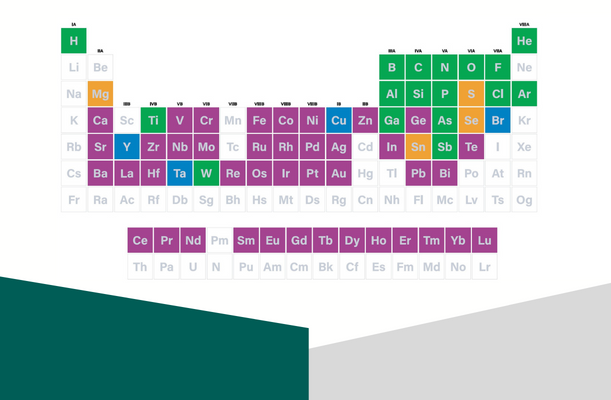
“Only about 25 years ago, the number of materials that were important for microelectronics was very manageable,” says nanoelectronics professor Thomas Mikolajick of TU Dresden, outlining this trend. “Since then, that number has really exploded, and semiconductor technology has expanded to include a large part of the periodic table.” Among them are some elements and compounds on which the industry has particularly high hopes for the near future – here’s a little “tour d’horizon”:
Metal oxide semiconductors such as indium tin oxide (ITO) and indium gallium zinc oxide (IGZO)
They are considered to be the hope for the three-dimensional logic and memory circuits of the next generation but one. As transparent interconnect materials, they have already been in use for years in solar cell and display manufacturing, for example. However, these metal oxides are also suitable for the 3D CMOS concept. According to expert estimates, this will become the focus of the semiconductor industry in about five to ten years, when it is about to move into the sub-nanometer world. Then ITO and IGZO could provide the key to three-dimensional stacked transistor levels. 3D architectures already exist for individual transistors such as the FinFET or for memory in USB sticks, but not for complex logic circuits. The technologies are being researched primarily by Imec in Belgium, but also by TU Dresden.
Advantage
.
- Can be processed at low temperatures – important for the layered structure!
Disadvantage
- Unlike silicon, these metal oxides are not single crystals, their charge carrier mobility is lower – meaning: possibly it will be harder to achieve high switching speed
.
Applications
.
- Originally integrated electronics for autonomous cars, smartphones, data centers, control electronics in factories, etc.
Magnetic stacks with materials such as cobalt-iron-boron or iridium-platinum compounds, magnesium oxide etc.
They are expected to enable cheaper and more powerful memory cells.
Advantages
.
- fast storage capability
low voltage
.
Disadvantages
- Separation of materials is laborious and expensive
Industry still has little experience with it
Applications
- Memory cells embedded in logic circuits or other complex systems
Tantalum oxides and amorphous hafnium oxide
.
They are suitable for memristors. These are electronics that “remember” previous states, so in a sense “accumulate experience.” Panasonic and TSMC already produce such memories.
Advantage
.
.
Disadvantages
- Can only withstand a relatively low number of switching cycles
Industry still has little experience with it
.
Applications
- Currently in demand primarily as a low-cost alternative to flash memory cells
Prospectively as hardware for certain artificial intelligence (AI) computing tasks
Crystalline hafnium oxide
… in its orthorombic version (crystal with three perpendicular axes) is a ferroelectric material and a hope for fast memory and AI hardware. The breakthrough was achieved mainly in Dresden: once at Qimonda and then at the TU’s NaMLab, Fraunhofer CNT and the “NaMLab” spin-off “FMC”.
Advantages
- As memory in performance and efficiency a quantum leap compared to flash
- Easily integrated into existing CMOS processes
.
Disadvantages
- can only tolerate a few million switching cycles
- relatively high voltage (about 3 volts)
compared to MRAM.
Applications
- very fast memory with very low power consumption
- perspective: neuromorphic computing for artificial intelligence
Silicon carbide and gallium nitride
.
Both are semiconductors with a high band gap between the outermost electron bands. As a result, they can tolerate higher voltages and stronger currents than ordinary silicon devices and resist current less. In Saxony, the X-FAB -Werk in Dresden, among others, manufactures gallium nitride semiconductors.
Advantages
.
- High reverse voltage up to several thousand volts
- Little resistance when switched on
- Tolerates high currents
.
Disadvantages
- more complex technology than silicon
- doping is challenging
- crystals are difficult to grow – hence, with gallium nitride (GaN), mostly layer buildup on silicon wafers
so far.
Applications
- Latest generation power electronics, for example, rectifiers and inverters in solar and wind power plants, transformers and other power systems, power supply devices for consumer electronics, electric rail vehicles
- GaN is also suitable for high-frequency technology in “High Electron Mobility” (HEMT) transistors
.
Gallium Arsenide
Gallium arsenide has been used for years in high-frequency
quence electronics. Its use as a material for power electronics is still quite new. It is conceivable that it could be used to cover a niche between silicon in the lower power spectrum and silicon carbide or gallium nitride on the other side. Saxony is considered an important location for gallium arsenide semiconductor technology. Among the pioneers here are Freiberger Compound Materials (FCM) and “3-5 Power Electronics” from Dresden.
Advantages
.
- larger band gap than with silicon
- higher charge carrier mobility with silicon – thus high switching speed possible
.
Disadvantages
- More complex technology than silicon
.
Applications
- In addition to the classics such as LEDs and high-frequency technology, power electronics diodes have also come into view, for example for electric car charging stations
Gallium oxide
Gallium oxide could enable the next generation of power electronics after silicon carbide and gallium nitride. However, this technology is still in the research phase.
Advantage
.
- Would tolerate even higher voltages and stronger currents. Reason: the band gap between valence and conduction electron bands here is 4800 electron volts (eV), even larger than silicon (1100 eV), gallium arsenide (1400 eV) and even than gallium nitride (3000 eV)
.
Disadvantage
.
- Not yet a ready-to-use technology
.
Application
- Next generation power electronics
Conclusion
.
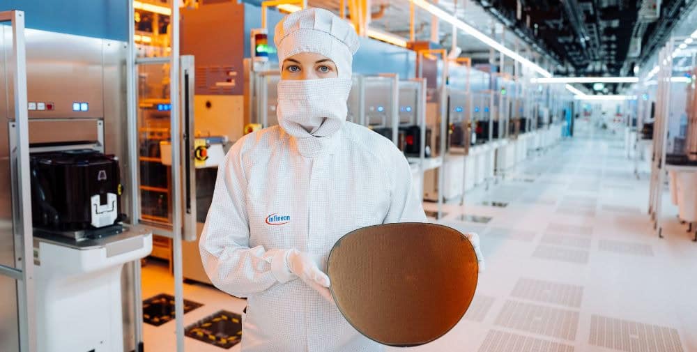
High-tech companies and research institutions in Saxony are working on several of these promising material developments. One particular focus is on power electronics, among other areas. Lighthouses in this segment include, for example, a gallium nitride research center in Freiberg and Freiberger Compound Materials (FMC), as well as TU Dresden’s NaMLab, Infineon’s power electronics production, X-FAB’s gallium nitride line in Dresden and others.
This article first appeared as part of our NEXT magazine, “In Focus: Microelectronics.”
👉 Go to the full issue of the magazine